Technology deep dive
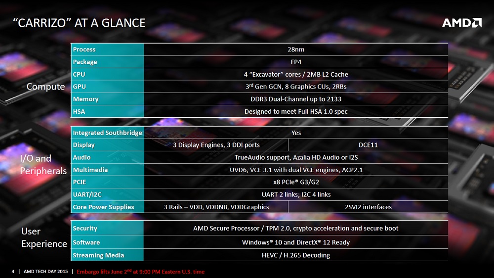
AMD's feature set and strategy behind Carrizo is coherent enough but let's take a closer look at the technology which underpins it. From a high-level overview Carrizo is AMD's most advanced APU with 30 per cent more transistors than mobile Kaveri within the same die area and on the same 28nm process. The use of the 28nm process was described by AMD as a strategic and cost-based decision, 28nm allows them to maintain an optimal balance between cost, performance and architectural complexity.
The Excavator CPU
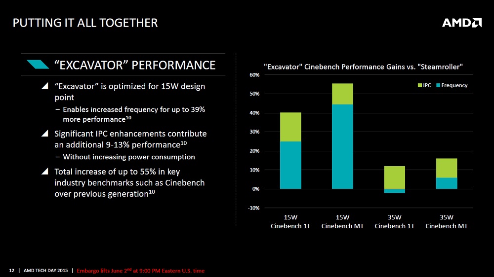
Carrizo makes use of the last CPU architecture in the Bulldozer family, Excavator. The fundamental design advantages of Excavator compared to previous-generation Steamroller are improved instructions per clock to the tune of 4 to 15 per cent, new instruction support, a smaller size footprint and reduced power consumption..
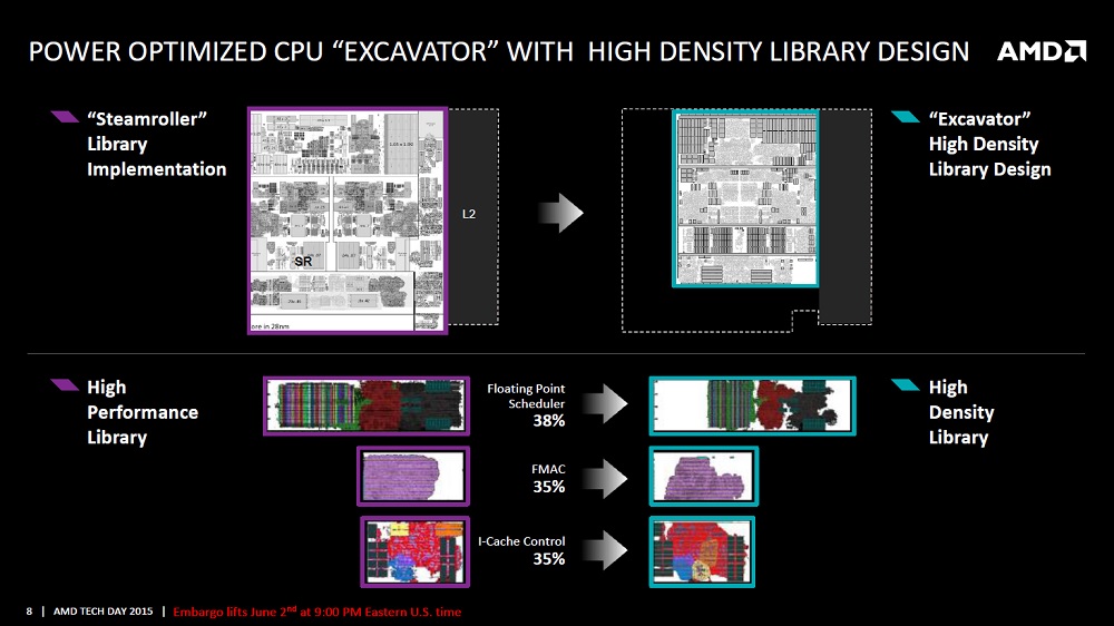
To achieve a smaller size footprint AMD used algorithmic allocation for the Excavator library, this compares to the Steamroller library which had many "hand drawn" parts that were less space efficient. The end result is a smaller and higher-density design which is more power efficient, though some trade-offs are made to achieve this. Excavator starts to drop off in frequency, compared to Steamroller, when moving beyond the optimised 15-watt envelope. Such a drop off is likely why the consumer market may not see a high performance desktop design - Carrizo may not be able to reach those 65-watt and 95-watt performance segments in its current high-density form.
Power savings on the CPU side have been primarily achieved through two methods. Firstly, through advanced power gating and power management that ensures unused transistors and other CPU components are shut down when not in use, even if that is only on a nano- or micro-second time scale. Secondly, the Carrizo APU makes use of independent voltage planes so that different hardware components can be turned on and off independently of others.
More to that point Carrizo now has three separate input voltages, with respective sub-voltages for each - one for the FCH, one for the CPU and one for the graphics. This allows for finer tuning of power consumption for different workloads depending on its specific hardware requirements. In tandem with the decision to integrate the chipset onto the APU die AMD has managed to reduce overall idle system power by around 40 per cent allowing AMD to take a large stride towards its 25x20 objective
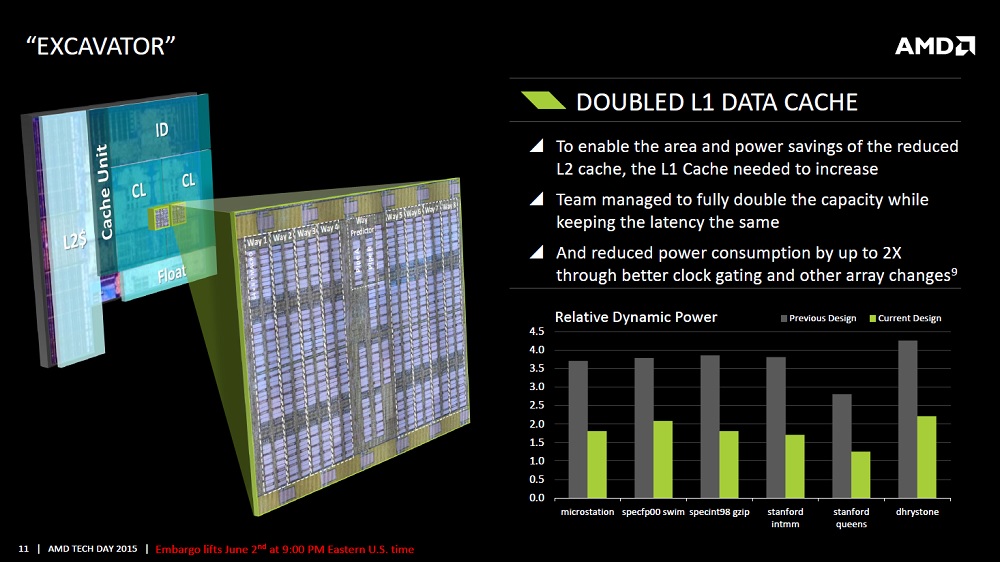
On the performance side AMD has managed to increase instructions per clock using a number of tweaks. The L1 data cache has been doubled without increasing latency, although, the company did note that some of the performance gain from this is counteracted by a reduction in the size of the L2 cache, a move intended to reduce power consumption. Better branch prediction techniques, thanks to a larger buffer, and improved prefetch techniques have also contributed to IPC increases. AMD's own internal figures reveal that the greatest performance increases have been achieved in the 15-watt envelope and in multi-threaded workloads while the performance gains are lesser at the 35-watt level.
Dedicated Video Hardware
As part of AMD's plan to target entertainment streaming workflows the dedicated video hardware plays an important role. In a typical playback scenario the GPU is tasked with scaling and processing images for the video but using a new "underlay" video playback path, which uses a dedicated video processing pipeline between the Universal Video Decoder (UVD) and display, the Carrizo APU can skip the GPU to save 0.5-watts of power. Even without the underlay method Carrizo is able to use less power than Kaveri in 1080p video playback.
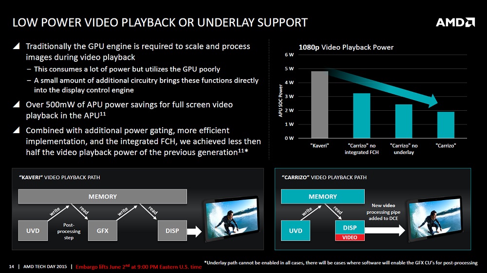
The revised UVD on Carrizo has four times the decode bandwidth of Kaveri allowing workloads to be completed four times quicker. With the extra time AMD has programmed the UVD to power gate and put DRAM into a low power state to consume less power. In total there's a power reduction of around 50 per cent when playing back 1080p video resulting in enhanced battery life for media-centric users. The AMD UVD supports six major video formats - H.265/H.264, 4K MJPEG, VC-1/WMV profile D, MPEG-2, Multi-View Codec (MVC) and MPEG-4/DivX.
The 3rd Generation GCN GPU
Since the first launch of AMD's Graphics Core Next (GCN) architecture we've observed three revisions. GCN 1.0 was the first wave that included the HD 7970, GCN 1.1 included the new flagship R9 290X and GCN 1.2 was spearheaded by the R9 285. The Carrizo APU uses a similar GCN 1.2 "third generation" design as the R9 285 which includes improved tessellation capabilities and lossless delta colour compression.
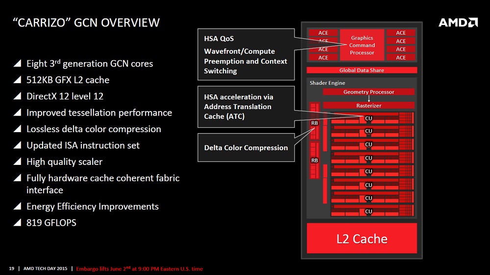
As part of the full HSA 1.0 compliance the Carrizo GPU has support for HSA acceleration features like Address Translation Cache (ATC) and Quality of Service (QoS) scheduling support. There is increased coherence between system memory and the CPU and GPU cache which helps to boost memory bandwidth, an important consideration given that APU graphics have been limited by slow system memory thus far. An improved Carrizo display engine, with a dedicated hardware block, also allows for up to 4K resolution support and an improved downscaling method.
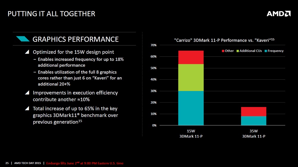
By deploying the dedicated voltage plane and using a higher-density design AMD has been able to enable all eight compute units (CUs) on Carrizo in the 15-watt envelope and at a higher frequency. The end result for performance is up to 65 per cent extra from a combination of additional compute units, higher frequency, the lossless delta colour compression and other minor design tweaks that increase execution efficiency.