Westmere to come in early
Tell me about Westmere
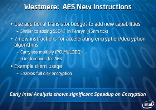
Westmere encapsulates the bulk of the Nehalem architecture, on a smaller, cheaper-to-produce 32nm process, but adds a few new tricks, including seven new instructions to the SSE set that focus on CPU-accelerated, hardware-based AES encryption and decryption at 3x the speed of Nehalem. As the slide shows, it'll be handy for large-capacity disk encryption.
The 32nm process is based, in part, on immersion lithography, as used by AMD on 45nm, and it works by increasing the resolution of the lithography between mask and wafer by adding pure water in between. The extra resolution helps bridge the gap between 45nm and 32nm nodes. Upfront costs are higher for equipping to an immersion process, but Intel is shelling out some $7bn in equipping US fabs with the tools required for a smaller process.
Pragmatically, a 32nm node means that Intel can produce more chips per given wafer, decrease voltage of NMOS and PMOS transistors, and, well, yield at higher frequencies. That's the theory, anyway.
Think of Westmere as Nehalem with cherries on top, folks.
Pooof: 45nm disappears before your very eyes
Looking at Intel's desktop roadmap, as disclosed in August 2008, we see the following:

Generally confusing because of code-names, there is no mention of 32nm Westmere, as all projected platforms are based on 45nm Nehalem derivations, from Core i7 at the top to dual-core Auburndale, centred around mobile, at the bottom.
However, tellingly, Intel is demonstrating working 32nm (Westmere, if you need reminding) samples today, in both desktop and mobile form, intimating that it's well ahead of disclosed schedule.

Here's a high-level view of the current roadmap, presented today by Stephen L. Smith. What we see is that 32nm Westmere is being brought in around one quarter before expected, late on this year, and it has some important ramifications, as well.


