APU 2014 - Part I
Abridged history of APUs
AMD has been steadily improving its premium Accelerated Processing Units (APUs) since the inception of the Llano processor in June 2011. The first-generation APUs integrated AMD's K10 CPU and Radeon HD 5000-series discrete graphics on to a monolithic die, thus enabling mainstream desktop and laptops to be powered by a single processor.
A major APU update, codenamed Trinity, arrived almost a year later, this time imbued with updated technology for both the CPU and GPU in the form of Piledriver cores and Radeon HD 6000 graphics, respectively, though the newer CPU architecture was often slower than the one it replaced. AMD, however, cemented its position as provider of best-in-class graphics through improvements to the GPU. Moving on another year to Richland, considered a minor refresh, AMD's arguably kept ahead of Intel's recent APU-like Core i3 and Core i5 processors in the all-important bang-for-buck-metric... but the gap is closing.
The newest APU technology now resides in 'Kaveri'-based chips announced at the Consumer Electronics Show in January 2014. This time around and keeping up with the times, AMD fundamentally upgrades the graphics portion of the APU to the GCN architecture found in all the latest discrete Radeon GPUs and consoles whilst making incremental improvements to the CPU cores.
Brief APU comparison
APU Model |
Process |
CPU Cores |
CPU Tech |
Max CPU Clock |
GPU Cores |
GPU Tech |
Max GPU Clock |
AMD Turbo Core |
Form Factor |
TDP |
|---|---|---|---|---|---|---|---|---|---|---|
| Kaveri | 4 |
28nm |
Steamroller |
4.0GHz |
512 |
Radeon R7 |
720MHz |
Yes |
FM2+ |
95W |
| Richland | 4 |
32nm |
Piledriver |
4.4GHz |
384 |
HD 6000 |
844MHz |
Yes |
FM2 |
100W |
| Trinity | 4 |
32nm |
Piledriver |
4.2GHz |
384 |
HD 6000 |
800MHz |
Yes |
FM2 |
100W |
| Llano | 4 |
32nm |
Stars |
3.0GHz |
400 |
HD 5000 |
600MHz |
No |
FM1 |
100W |
The high-level overview shows the key performance attributes of each AMD APU series. Let's take the improvements turn by turn and thus evaluate whether Kaveri APUs offer a worthwhile upgrade over last-generation Richland.
28nm, does it matter?
AMD's move down to a specific 28nm fabrication process has ramifications for the Kaveri APU beyond that of a smaller die. Joe Macri of AMD explained that previous APUs used silicon that was designed for frequency above denseness, a vestige of CPU design, thus optimising for MHz above parallelism by using speedy, low-metallised transistors. Now, as the GPU becomes more important - 47 per cent of the Kaveri die is devoted to it - and power is of greater concern, AMD, in conjunction with GlobalFoundries, is using an 'APU-optimised' process that offers a better compromise between all-out speed and ability to make the APU's compute more parallel.
There are two key upshots from this. Firstly, the need to find a happy medium between performance, power and parallelism means this 28nm Super-High-Performance (SHP) process doesn't have the ability to scale the cores as high as on previous APUs. We can see this by looking at the maximum speeds of both; the peak frequencies of the CPU and GPU parts is lower than Richland on a roughly-equivalent TDP. But secondly, use of 28nm SHP also allows AMD to shoehorn 512 graphics cores, which is comfortably higher than on any previous all-in-one processor. AMD's adamant that this balanced design and wide dynamic range - the architecture has to fit into 15-95W TDPs - wouldn't have been possible without the substantial tweaking undertaken here.
And it's a big chip, too, weighing in at 2.41bn transistors, or over 1bn more than Trinity/Richland that it replaces. The AMD APUs share a die size of around 245mm², so not only does the 28nm process offer improvements in terms of gaining parallelism, it is very much needed in order to keep manufacturing costs sensible. As you can imagine, most of this extra transistor budget is for the graphics cores.
The steamin' CPU cores
AMD is introducing a new CPU technology for Kaveri APUs. Known as Steamroller and an enhanced, improved version of the Piledriver core present in both previous-generation APUs and discrete FX CPUs, this latest technology is a good fit for cutting-edge processors.
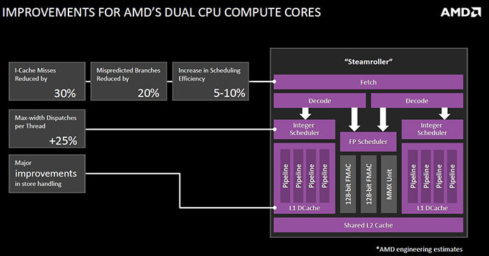
Getting granular, Steamroller is an enhanced version of the Piledriver core, just as that was when compared to the original Bulldozer found in the first-generation FX chips. The basic architecture topology remains intact, yet AMD has made some key changes with respect to efficiency, particularly at the fetch and decode stages of the pipeline, in an effort to boost throughput by reducing bottlenecks and stalling at the start of the compute process.
Getting more granular, the instruction cache has been boosted by 50 per cent, to 96KB, reducing misses by up to 30 per cent. The extra cost of silicon is worth it, says AMD, because misses here really hamper pipeline execution. Missing branches are also costly when processors become more parallel, so AMD doubles the branch target buffer. The scheduler, too, is improved, with Steamroller upping Piledriver's 40 entries to 48. More is better because a wider scheduler enables the chip to be fed with instructions to a higher degree - efficiency by a different name.
There are also two distinct integer schedulers and ability to issue two stores at once, compared to one in the previous generation on each count. Looking at the backend, access to memory is improved by deepening the queues for load/stores, meaning that Steamroller can jump between main memory and the chip's registers more quickly than either Richland or Trinity.
What does all of this mean in terms of real-world processing? AMD believes the improvements add up to an average 10 per cent uplift over Piledriver-based Richland in instructions-per-cycle (IPC) throughput, peaking at 20 per cent for best-case scenarios. The uptick is decent from a generation-to-generation point of view.