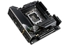
Interview with Albert Chang, Division Director of ASUS Motherboards

Albert Chang is the Division Director of ASUS Motherboard and Desktop R&D Department. He shares his thoughts on what makes the ASUS OC Socket unique, compelling, and a must-have feature on Intel X99 motherboards.
For enthusiasts who aren't aware of OC Socket, explain in a nutshell why it should matter to them?

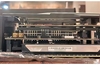
AC: ASUS has exclusively developed the OC Socket with extra pins beyond the standard LGA2011-3 socket on X99 motherboards. During overclocking this delivers improved stability when adding voltage, allowing overclockers to push the new Core i7 5960X, 5930K and 5820K CPUs to their absolute limits.
And it also allows for significantly improved DDR4 memory overclocking performance and bandwidth, compared to boards with a standard 2011-3 socket. The OC Socket design is only one part of the whole system, but it’s so important we’ve patented it (patent-pending) to protect our investment in R&D, and ensure the advantage for ASUS and ROG fans.
What encouraged ASUS to develop the OC Socket?
AC: When we began the X99 project we quickly discovered that the number of CPU pads exceeded the number socket pads, so we set out to discover this undocumented feature. We expended considerable R&D effort to discover the functions of the extra pads, and apply them to our layout design and UEFI BIOS. The OC Socket was then created to bridge the gap between CPU and motherboard design.
So while we refer to this innovation generally as “OC Socket”, it is much more than a simple change in socket pin layout. It is in fact part of a much larger design effort.
In your opinion, what are the three most important benefits to the OC Socket over regular LGA 2011-3?
- Higher memory frequency with low memory voltage.
- Access to cache bus voltage to boost cache bus frequency. This greatly improves memory read/write performance, which translates into real-world benefits for memory intensive applications.
- Monitor and control specific CPU cores. Perfect or overclockers who want to isolate their best CPU cores.
What other PCB innovations did ASUS need to create in order to maximise the use of the OC Socket?
AC: While we cannot divulge specific designs, we have optimized the PCB layout to suit the OC Socket, using an advanced T-Topology DDR4 memory design to improve memory frequency scaling and performance. The OC Socket, PCB layout optimizations, and an advanced UEFI BIOS all need to work together to get the best results.
OC Socket promises improved DDR4 performance - how do extra socket pins help with memory overclocking?
AC: The key is the unique cache bus voltage adjustment. The cache bus links together areas such as the CPU cores, DDR4 memory controllers, System Agent and the shared L3 Cache. A higher cache bus frequency directly correlates to faster total sub-system performance. OC Socket provides an adjustable cache bus voltage to reach higher cache bus frequencies. From our UEFI BIOS, you can see that the ASUS OC Socket tuning ratio range is over 45x or even 50x, while the Intel reference tuning ratio range is only up to 30x.
OC Socket is currently available exclusively on X99 boards, is ASUS actively investigating similar enhancements on other, more mainstream Intel sockets?
AC: For every generation, ASUS will customize and develop the optimal design and features required to unleash the maximum performance from the platform. It is our passion to design and implement new and innovative features in all our products, so that our customers can enjoy unique benefits from ASUS hardware. However, the origin of OC Socket is down to the discovery of the additional contact points on the CPU, so if the number of CPU pads matches the number of pins in the socket, there is no scope to create an OC Socket design similar to that on ASUS X99 boards.
While the OC Socket is a patent-pending design, what's to stop other manufacturers from implementing similar functionality?
AC: The OC Socket total design is patent-pending, and we have done this in order to protect our considerable investment in research and design. However, should anyone attempt to circumvent the patent, they would need to commit many months of R&D effort into PCB layout, UEFI design and validation in order to even attempt to match our complete package of performance and quality.
Concerns have been raised over whether or not the use of OC Socket would void the warranty on Intel Haswell-E CPUs. Is there any truth to those claims?
AC: It has already been confirmed that OC Socket does not void the CPU warranty. The ASUS OC socket is slightly different from the reference LGA2011-3 socket in that it has more pins, but these pins only activate when the CPU is overclocked. Under normal circumstances they are not active, and so the OC Socket operates no differently to a standard 2011-3 socket. Also, normally when you start overclocking, your warranty from Intel is automatically void anyway. So in reality there is no difference.
How has Intel reacted to ASUS creating a customised socket, and has the chip giant been supportive in the development of OC Socket?
AC: Our relationship with Intel is always very strong and positive. We work closely together, but we also have a history of offering more capability and flexibility on our boards, to push the very limits of a PC platform. The OC Socket is an ASUS feature that is based on the Intel reference design, and we developed and validated this feature. This is no different to other features, such as our unique power design, memory topology and UEFI BIOS, all of which deliver greater value and performance to our fans and customers.
It surely won't be long until rival boards arrive with their own take on OC Socket. When that happens, how will ASUS keep ahead of the pack?
AC: Should anyone attempt to circumvent the patent, they would need to commit months of R&D efforts in PCB layout, UEFI design and validation efforts to even attempt to match our complete package of performance and quality. Due to ASUS’ unrivalled technical expertise in motherboard hardware and UEFI design, we are confident that even if a rival socket did appear, the ASUS OC Socket, combined with all our other innovations, such as power design and UEFI design, would still deliver the best very blend of performance, stability and reliability.