


Layout
Click for a bigger version
Click for a bigger version
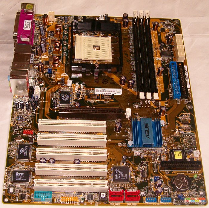
The layout isn't too different to the K8V, and that's a very good thing. While the nForce3 250Gb core logic is implemented in a single ASIC, meaning the board space used by the K8V's southbridge is usable by something else on the K8N, the basic layout traits of the K8V are carried over.
The ATX12V connector is the first major board component to be found from examining the layout as presented above, going from left to right, top to bottom. The K8N uses 3-phase power delivery for the CPU. ASUS orientate the socket west-to-east on the K8N, with the standard Socket 754 CPU retention mechanism keeping the socket area free and clear of any potential impingements. After that, we hit the three DDR DIMM slots that give the K8N its 3GB max memory support. ASUS recommend you start with the DDR slot nearest the CPU when populating the board with DIMMs, if you're not using the full three slots provided.
After that we have the IDE ports connected to the 250Gb ASIC, along with the main 20-pin ATX power connector, sensibly placed on the outer edge of the PCB.
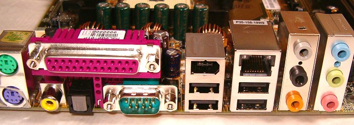
Under the CPU socket, before the AGP slot, you'll find the two SATA ports that connect to the 250Gb, along with the Marvell Alaska PHY transceiver for the Gigabit Ethernet port, again connected to the 250Gb. The AGP slot is next, just far enough under the DIMM slots such that longer AGP graphics cards can be installed and kept there, even if you wish to change your memory configuration.
Five PCI slots flank the 250Gb bridge, passively cooled by the usual blue ASUS aluminium heatsink that'll you'll see on K8V, SK8V and SK8N.
The floppy port sits east-west oriented in the bottom right hand corner of the board, a less than optimal orientation, but in roughly the right place on the board.
That leaves the Sil3114 and its four, red SATA ports at the bottom of the board to round out the important parts of the K8N's layout. The Sil3114 ports would be better placed if they could swap places with the floppy port and the BIOS chip, in this reviewer's opinion at least, due to SATA data cable length restrictions, but they could be sited a lot worse.
A decent layout, carrying over the fine properties you can find in K8V, but not without its little niggles. Could be better, but also a hell of a lot worse.


