


A New Generation of GeForce
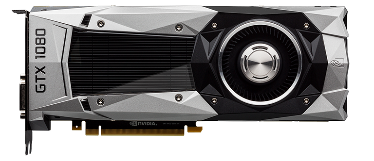
The wait is finally over as Nvidia has unveiled the eagerly anticipated GeForce GTX 1080 graphics card.
Launched as a successor to the hugely popular GeForce GTX 980, the new GPU slots in at the top of Nvidia's consumer lineup and touts a number of revolutionary performance enhancements for enthusiast users. Chief among these is the introduction of a brand-new architecture, codenamed Pascal, that promises a significant speed-up against the GeForce GTX 980 from 18 months ago. Nvidia reckons it's 25 per cent faster than even the Titan X for regular gaming and, crucially, up to 2x speedier for virtual reality.
So how has Nvidia managed to beat its best card from last year, handily so in many cases, when using about 30 per cent less board power and a die that is roughly half the size? The devil, as always, is in the details, and GTX 1080 combines a number of cutting-edge benefits to boost efficiency to levels not seen before in the high-end gaming space. If you only take away one morsel of information from the introductory pages, it should be that efficiency, rather than brute force, is what drives the GTX 1080.
Improvement #1 - 16nm FinFET Transistors
AMD debuted the Radeon HD 7970 in December 2011. Nvidia rolled out the GeForce GTX 680 in March 2012. Both of these two high-end GPUs were special insofar as they were manufactured on a 28nm process. The subsequent four years have seen numerous GPUs come and go, often equipped with new architectures and clever technology, yet the transistors they're built on have remained constant.
That changes today. Nvidia is the first to move to a 16nm transistor-gate process built by TSMC, leapfrogging the ill-fated 20nm node that was due last year. Putting it simply, having smaller transistors enables more to be packed into a given area, minimising die space and therefore ensuring that more are produced per silicon wafer. What's more, less voltage is required to drive each transistor, reducing overall power consumption or, if you look at it differently, offering more scope for turning up the speed.
The actual economics of it aren't this simple, of course, as moving down nodes/processing has an ever-increasing implementation cost, but the overall benefits of the process continue to outweigh the per-mm² price; the up-front outlays are amortised over the length of the process, so expect 16nm to be around a while for graphics. The technology isn't that simple, either, as packing in ever-denser transistors can lead to huge leakage through a phenomenon known as quantum tunnelling while short-channel effects become more prevalent as we move processes.
These electrical problems have been satisfactorily solved by foundry partner TSMC, who also builds 16nm parts for other companies. 16nm, then, is a good thing. If implemented correctly, it offers excellent die-space characteristics, drops power consumption and/or increases speed.
The GeForce GTX 1080 puts these enviable properties to good use. The GPU packs in 7.2bn transistors - a goodly amount for a high-end graphics processor - into a die area of just 316mm². We'll get on to inter-generation comparisons in a mo', but it's worth pointing out that the best Maxwell GPU used 8bn transistors in a 601mm² die and the premier Kepler, also on 28nm, 7.1bn in 561mm². In other words, from a pure process point of view, ignoring all architectural benefits, Nvidia is saving around 45 per cent die space.
Of course, we're not comparing absolute like for like, as the GeForce GTX 1080 doesn't use the full force of Pascal architecture - the Tesla P100 has that honour - yet it's clear to see that, should Nvidia so choose, it can price the card very aggressively.
Improvement #2 - Memory: GDDR5X and New Compression
Resolution and image quality have been the main catalysts for games looking more realistic than ever before. Sensible GPU design predicates that as much computation is kept on the processor as possible, minimising the need to load data from main memory, which is an order of magnitude slower than the various caches on the GPU.
The largest cache on a GPU, by some distance, is the framebuffer from where various algorithms work on the data to increase visual fidelity - antialiasing and filtering, for example - and from where the final frame is transported out to the display. You want this framebuffer to be as large, fast and low-latency as possible, especially when turning the image knobs up to 11. Kind of makes implicit sense, huh?
Nvidia's engineering team, headed by senior vice president Jonah Alben, had an obvious design decision to make for GTX 1080. They could have tried to implement high-bandwidth memory (HBM), as AMD did for the Fury X graphics card. HBM is the future; it offers super-wide access allied to low power and reduced physical footprint, and it's present on the Tesla P100 variant of Pascal. However, HBM is currently limited in capacity, production volume, and is difficult to implement quickly. HBM 2 is likely to solve a couple of these problems.
More bandwidth is almost always better, so the Green Team could have chosen to keep the 384-bit bus present on GTX 780 Ti/980 Ti and run regular GDDR5 at 7Gbps, serving up 336GB/s of bandwidth. Such an approach would have worked well enough, we imagine, though Nvidia chose to use a narrower 256-bit bus which saves on both power and transistor count. Question is, how can you use a comparatively narrow bus without sacrificing on usable bandwidth? The answer comes in two parts.
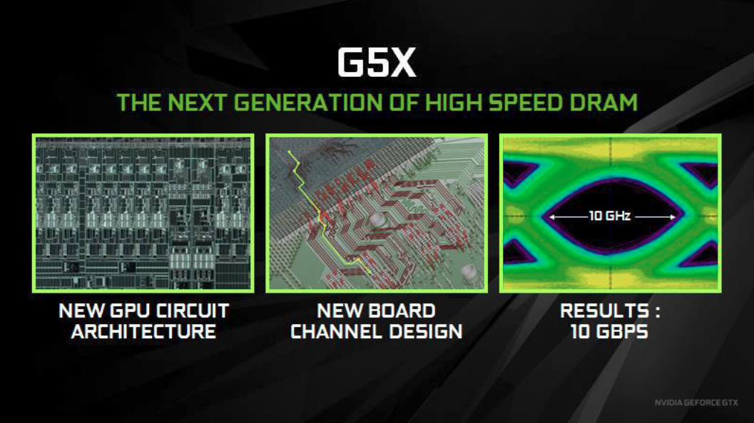
Nvidia, in conjunction with Micron, has developed what it calls GDDR5X memory. The high-level architecture is the same as incumbent GDDR5. The X variant can be thought of as a highly tuned spin-off of GDDR5, and the two companies say that every portion of the GDDR5 architecture was analysed to see if extra performance could be eked out. A new IO circuit was developed for this very purpose along with a new GPU-to-memory interconnect. This means GTX 1080 uses brand-new physical layers on the chip itself. GDDR5X also drops power from 1.5V to 1.35V, resulting in the same power consumption at a 43 per cent higher frequency, according to Nvidia.
The upshot of this technology, which appears to be Nvidia-specific for the time being, is memory operating at an effective 10Gbps whilst using no more power than traditional GDDR5 at 7Gbps. The company has kept the entire memory subsystem small (256 bits) and fast. There's a potential 320GB/s, closely matching the overall bandwidth previously offered by a wider, slower bus that takes up more die space. What's clever is that the learnings from GDDR5X will be reused with regular GDDR5. In other words, expect future cards of this generation to offer 8Gbps-plus.
Yet considering bandwidth from a pure numbers point of view can be misleading because it doesn't take newer memory-compression technologies into account. AMD and Nvidia have both improved lossless memory compression over subsequent generations, meaning that an effective 7Gbps today is not the same as that from, say, 2013.
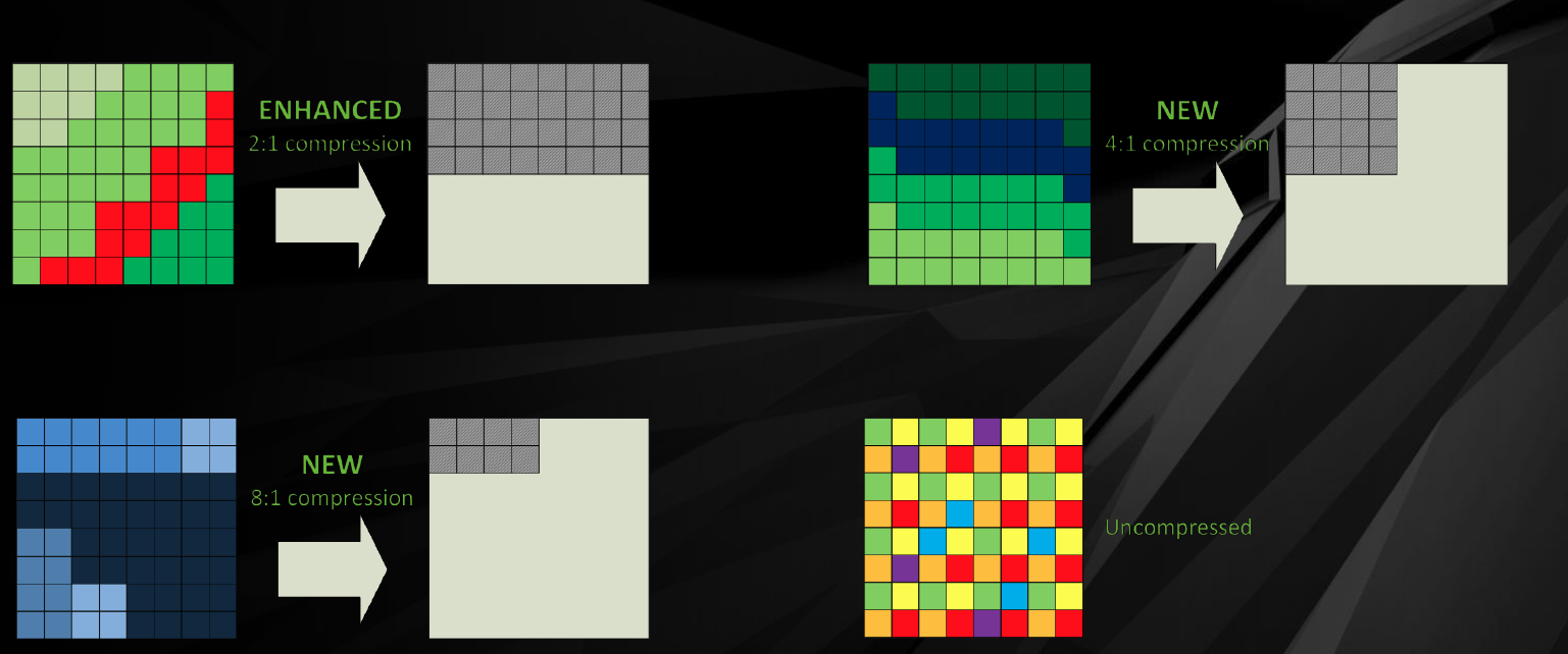
The latest compression technology from Nvidia enhances what's available from Maxwell. All modern GPUs use some form of lossless compression to minimise the amount of data written out to memory, saving power and keeping performance high. Colour compression, as the name suggests, examines a frame and determines how many 2x2 pixel regions share the same colour. If they're exactly the same, they can be compressed on an 8:1 basis. If not, lower compression is considered.
Delta colour compression examines blocks of pixels and evaluates the difference between the two. Similar blocks have fewer differences and therefore less data needs to be written out across the bus and caches. Algorithms manage how this compression/block similarity is processed.
Now, there's an intermediate mode called 4:1 compression. It improves upon Maxwell by compressing colours that are very close to one another, but not exactly the same. The 8:1 compression has also been improved because it now, on top of the 4:1 constant colour compression, also uses a 2:1 compression of the delta between the blocks. Think of this as an upgraded version of the usual technology.
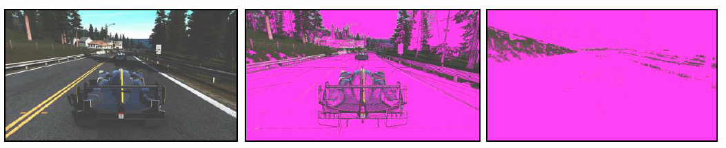
Here's an Nvidia-provided screenshot showing the level of memory compression on Maxwell (middle) and Pascal (right). Anything not pink hasn't been compressed, and it's patently clear to see, on this example at least, the extra efficiency that leaves greater bandwidth available to the GPU. The ability to compress near-identical colours pays dividends when looking at the foliage on either side of the car; Pascal's enhanced technology all-but eradicates the right-hand side.
We know that compared to GTX 980 there's 40 per cent more bandwidth through a speed-bump to the memory. Nvidia reckons the enhanced compression adds another 20 per cent or so, evaluated over a number of games, so actual effective bandwidth is closer to 70 per cent.


