


Introduction
GPU architectures tend to run like London buses - you rarely see a new one and then, quite unexpectedly, two come along at once. Curiously and interestingly, Nvidia and AMD debut their premium graphics GPU architectures within a month of one another. Thinking about buying a really good graphics card right now? Read away.
Let's make something clear at the very outset of this review. The two GPU heavyweights have decided to use a different tack towards solving the problem of gaming at high resolutions. These decisions are actually made some time in the past, often years ago, so what you see today is the engineering teams' design ethos back in 2012 or so.
Nvidia teases out iterative gains from the energy-efficient Maxwell architecture and relies on pushing considerable throughput on a 250W design. AMD, on the other hand, refines its GCN architecture and, instead, puts more focus on the memory side of things. We know all about Nvidia's efforts from looking at the impressive numbers posted by the GeForce GTX Titan X and, more recently, GTX 980 Ti, so let's examine how AMD goes about letting loose a behemoth of a GPU: enter the Fiji-infused Radeon R9 Fury X.
AMD is telling the Fiji story in bite-size chunks. First came details about an innovate, clever new technology called high-bandwidth memory (HBM) - more on this later. Next came the partial reveal at last week's E3 show, with senior AMD representatives offering glimpses into the card's performance. Part of that reveal was disclosure of the Fury X's high-level specs.
Radeon R9 Fury X |
Radeon R9 390X |
Radeon R9 290X |
GeForce GTX Titan X |
GeForce GTX 980 Ti |
GeForce GTX 980 |
|
| Launch date | June 2015 |
June 2015 |
October 2013 |
March 2015 |
June 2015 |
September 2014 |
| Codename | Fiji XT |
Grenada XT |
Hawaii XT |
GM200 |
GM200 |
GM204 |
| DX support | 12.0 |
12.0 |
12.0 |
12.1 |
12.1 |
12.1 |
| Process (nm) | 28 |
28 |
28 |
28 |
28 |
28 |
| Transistors (mn) | 8,900 |
6,200 |
6,200 |
8,000 |
8,000 |
5,200 |
| Approx Die Size (mm²) | 596 |
438 |
438 |
601 |
601 |
398 |
| Full implementation of die | Yes |
Yes |
Yes |
Yes |
No |
Yes |
| Processors | 4,096 |
2,816 |
2,816 |
3,072 |
2,816 |
2,048 |
| Texture Units | 256 |
176 |
176 |
192 |
172 |
128 |
| ROP Units | 64 |
64 |
64 |
96 |
96 |
64 |
| Peak GPU Clock/Boost (MHz) | 1,050 |
1,050 |
1,000 |
1,076 |
1,076 |
1,216 |
| Peak GFLOPS (SP) | 8,602 |
5,914 |
5,632 |
6,611 |
6,060 |
4,981 |
| Peak GFLOPS (DP) | 537 |
739 |
704 |
207 |
189 |
156 |
| Memory Clock (MHz) | 1,000 |
6,000 |
5,000 |
7,012 |
7,012 |
7,012 |
| Memory Bus (bits) | 4,096 |
512 |
512 |
384 |
384 |
256 |
| Max bandwidth (GB/s) | 512 |
384 |
320 |
336 |
336 |
224 |
| Default memory size (MB) | 4,096 |
8,192 |
4,096 |
12,288 |
6,144 |
4,096 |
| Memory type | HBM |
GDDR5 |
GDDR5 |
GDDR5 |
GDDR5 |
GDDR5 |
| Power Connectors | 8+8-pin |
8+6-pin |
8+6-pin |
8+6-pin |
8+6-pin |
6+6-pin |
| TDP (watts) | 275 |
275 |
290 |
250 |
250 |
165 |
| GFLOPS per watt | 31.28 |
21.50 |
19.42 |
26.44 |
24.24 |
30.19 |
| Current price (Newegg) | $649 |
$429 |
$329 |
$999 |
$649 |
$499 |
Raising the table stakes
Fury X uses the full implementation of the so-called Fiji GPU die. Built on the same 28nm process that has been in evidence since December 2011, AMD doesn't tinker with the core architecture a great deal. Fury X uses the same GCN 1.2 blueprint - or third-generation iteration in AMD-speak - as found on the Tonga/Antigua GPU present in R9 285 and R9 380. Fury X's solution for meeting the high-resolution rendering problem head-on is more brutish than elegant: AMD scales up the design to accommodate more shading cores and texture units.
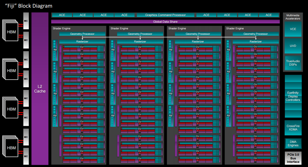
Whereas the nascent R9 390X and R9 380 have 2,816 and 1,792 cores split over 11 and 7 Compute Units, respectively, Fiji increases this to a mammoth 16. With 256 cores per CU, there's 4,096 of these ALU units on hand. Maintaining 16 texture units per CU throws up a GPU-wide 256. Prior knowledge of the peak 1,050MHz clock frequency translates to a monster-ish potential 8.6TFLOPS of compute on a single GPU, handily dwarfing anything seen before.
AMD runs with a 596mm² die, which is very marginally smaller than Nvidia's Maxwell GM200, but knows any GPU design, no matter how big, remains a trade-off. The company's focus on compute provides key insight into AMD's hardware strategy. It clearly sees compute power - loosely defined as the ability to paint lovely-looking pixels - as being vitally important to games designers, so a large portion of the die is devoted to the CUs.
The trade-off in this case is a lack of scaling on the render back-ends, which stay at 64, along with no obvious increase in the four geometry processors and associated hardware already available in Hawaii. What's more, being a gamer-centric card first and foremost, the extra silicon required to enable faster double-precision support is missing on Fiji - it can process double-precision at 1/16th of SP... or at a rate slower than 390X.
In very broad strokes we can say that games engines that overly rely on masses of geometry and simple operations such as final-output blending may find Fury X's architecture to be lopsided. Those that put the onus on the GPU's ability to actually shade those pixels, first and foremost, will take to Fiji. The real dilemma for any hardware architect is to predict where the bottlenecks are going to be in two or three years time: AMD and Nvidia's latest GPUs show somewhat divergent thinking - GTX 980 Ti, for example, is stronger on the backend; Fiji monsters the shaders.
Fitting more with, well, no more
AMD achieves a rather neat trick of cramming in almost 50 per cent more shaders and texture units without increasing the card's TDP... as compared to the power-optimised latest-generation Grenada core found in the R9 390X. The real question that needs answering here is how has AMD been able to do this? The answer comes in three parts.
Any newer iteration of a GPU takes advantage of recent technology that couldn't be integrated into the first generation. Fiji is a case in point. AMD takes much of the power-optimising know-how from its latest Carrizo APUs and brings it to bear on Fiji. The GPU has, according to AMD's David Nalasco, much better power gating (SVI2) than previous models, lending a hand to efficiency.
The way in which each card boosts to a certain frequency is, from what we can discern, more like Nvidia, where a certain combination of voltage and frequency points are defined by more than just a rigid curve. Now, each point is based on other factors such as temperature and quality of silicon, and this fine-grained control enables the Fury X to hit its maximum speed without unduly wasting voltage. This is also why AMD quotes an average power of 275W - each card is different in its electrical characteristics. The downside is that there will be more card-to-card variation, just as we see we recent Nvidia models.
Clever power management will only get you so far. A second part of the power-efficiency angle is in keeping power consumption in check by reducing temperature as much as possible. A basic rule of physics is that power consumption rises in concert with temperature increases even if no extra voltage is applied to the processor, and this is known as the Poole-Frenkel effect. Pertinently for Fury X, a GPU consuming, say, 300W at 95°C is likely to consume approximately 10 per cent less if at 60°C. Put simply, by keeping the card cool via watercooling AMD is able to reduce the TDP by a healthy margin.
AMD taps into this by equipping Fiji with an integrated radiator, pump and watercooler, much the same way it did with Radeon R9 295X2. Could this 275W GPU have been air-cooled at 300W? Absolutely, yet AMD plays on a third power-saving string with the use of HBM memory.
HBM, of course
We've covered HBM memory in adequate detail previously. In a nutshell, HBM uses significantly less power than GDDR5, enables higher bandwidth to be reached from a super-wide, slower bus that's connected to the GPU through dense wiring via an interposer. HBM, too, offers lower-latency access and a simpler integration to the core. AMD says that a reasonable amount of die area is saved by not having to construct a 512-bit GDDR5 bus, as found on the 390X.
Though HBM memory is full of lots of goodness - masses of low-latency bandwidth and a much, much smaller footprint on the board - there is one immediate catch. First-generation HBM is limited to four 1GB stacks constituting a GPU-wide 4GB. With Nvidia running 6GB and 12GB on its top-tier cards and AMD shoehorning 8GB of GDDR5 on the latest R9 390X and 390 cards, the marketing message behind 4GB in tenuous at best.
Modern games engines make liberal use of larger framebuffers when run at high resolutions and with all the candy on. Any memory requests that cannot fit into the card's framebuffer are actioned over the PCIe bus from main system RAM, which is an order of magnitude slower. This is why, on some mid-range cards, you see game judder along when such accesses swamp the card's buffer. More memory, in short, is good.
The graphics driver controls the memory management requests made by the games engine. AMD says it has devoted resources at ensuring that the Fury X's 4GB buffer is used as efficiency as possible at all times, though the company doesn't go into any more granular detail than that. 4GB, if managed correctly, is more than enough for today's games and tomorrow's, according to AMD's Robert Hallock.
Asked if AMD was concerned that a relatively meagre 4GB of HBM memory would prove to be a problem for the Fiji-based Fury X GPUs, Hallock responded with a resolute "absolutely not". We pushed him further and cited examples of recent titles that routinely breached the 4GB framebuffer barrier at a 4K resolution. "Go do your own testing on Fiji and see if the 4GB framebuffer is a cause for concern," Hallock responded.
The question of whether 4GB is enough on the top-end Fury X card is difficult to answer without having access to an 8GB model for a side-by-side comparison at a 4K resolution. We can, to some degree, indirectly infer whether the GPU appears to be stalling by looking at the time taken to produce the last one per cent of frames in a particular title, and we'll do just this in upcoming benchmarks.
Efficiency leads to performance
AMD is able to produce a large-chip die with a relatively modest average TDP of 275W because it uses three key technologies that all save wattage: refined power management, watercooling and HBM memory. Had these not been introduced at this time then Fury X would have consumed 375W or so - not impossibly high but not easy to cool, either.
Think of the Radeon R9 Fury X has a scaled-up version of the Tonga GPU that's already available. Imbued with the delta colour compression technology and armed with oodles of bandwidth from HBM memory, Fury X, it could be argued, has a surfeit of bandwidth. It's robust in sheer shader throughput, too, with 4,096 cores housed in the most complex die ever seen on a consumer graphics card.
There's masses of shading power, masses of real-world bandwidth, and a watercooled design that's supposed to keep the Fury X card nice and quiet. And, looking forward, performance in DX12 should be good because the API shares much of the learning AMD has already done with Mantel, including asynchronous shading - something the competition cannot do. Sounds like a winning formula, right?


