


Card appearance and thoughts
NVIDIA's G80 range currently comprises of two SKUS. The first, GeForce 8800 GTX, is, without doubt, the most advanced and, arguably, the fastest GPU available today. I'd urge you to head on over to our technical take and appreciate why it's so damn good. Retail examples start at around £375 and special editions, now overclocked, can be as much as £550 for a single card.For those folks whose budgets don't extend that far, NVIDIA also launched the GTS SKU, which takes most of the goodness inherent in the GTX model but slows things down a touch, which also results in a lower price.
GeForce 8800 GTS, then, is a bit less of everything when compared to its bigger brother. Reference-clocked cards run with 500/1200/1600 clocks, representing core, shader and memory speeds, respectively, down from the GTX's 575/1350/1800. Pure compute power is reduced too, with GTS offering 96 (6 x 16) stream processors compared with the GTX's 128 (8 x 16). The card's frame buffer also sees a chop to 640MiB from 768MiB and, finally, whilst the memory clock is slower, overall bandwidth is reduced further by utilising a 320-bit memory bus rather than the GTX's 384-bit.
That might read discouragingly but make no mistake, GeForce 8800 GTS isn't a souped-up 7-series card; its pedigree is pure 8800. The benefit to the consumer of NVIDIA's selective money-saving by reducing frequencies and working parts of the GPU is manifested in a lower street price that's sub-£300 in most cases. Still expensive, yes, but it's definitely next-generation architecture available today.
With all that firmly entrenched in your mind, let's take a look at ASUS' wonderfully named EN8800GTS/HTDP/640M.
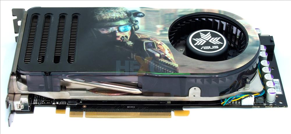
Informed readers will notice that the 8800 GTS' PCB is smaller than the GTX's, which we took a look at here. With the G80 core not running quite so quickly and memory speeds knocked down some, NVIDIA has been able to design in the necessary power regulation components without the need for an extra-long PCB. The heatsink itself, though, is virtually the same as the GTX's and, as such, the fan is virtually inaudible in 2D mode and very quiet when running the latest games.
We have to note that whilst the design is reference in all but the sticker on top of the card, ASUS is shipping its GeForce 8800 GTS cards with a slightly overclocked core, running at 513MHz as compared to the reference's 500MHz. That's good news for prospective purchasers as it amounts to a touch more performance for free. The memory clock, however, is reference, that is, an effective 1600MHz.
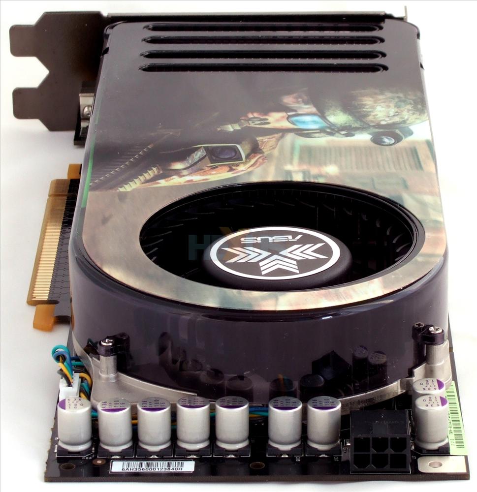
A look at the front highlights the lower power requirement of the 8800 GTS card; there's only a single PEG power connector present on the PCB.
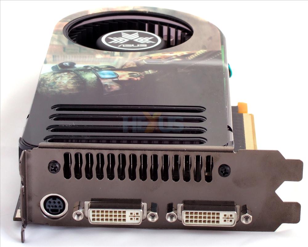
Intelligent HSF design means that the heat transferred from the GPU and memory chips is exhausted out of the back of the chassis. The heatsink's size, however, dictates that this GTS becomes a two-slot card, effectively blocking off the next slot down from your motherboard's x16 PCIe's. Both DVI ports are dual-link, meaning you can drive displays with extra-high resolutions without problems: 2560 x 1600 won't be a problem.
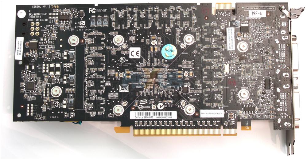
A look at the back serves only to highlight just how well-attached the heatsink is. Being a high-end NVIDIA card you can couple two together, via the SLI connector on the top-right of the picture, for multi-GPU love that is SLI. Just make sure your PSU has enough oomph to power them and the rest of the system. NVIDIA has a web page that lists all certified PSUs for SLI 'GTS usage.


