


Improving The Shader Units
In Nvidia's own words '...the SM scheduler architecture and algorithms have been rewritten to be more intelligent and avoid unnecessary stalls, while further reducing the energy per instruction required for scheduling.' The statement is a tacit understanding that Kepler's scheduler was likely overloaded and not entirely efficient when arbitrating between 192 cores.
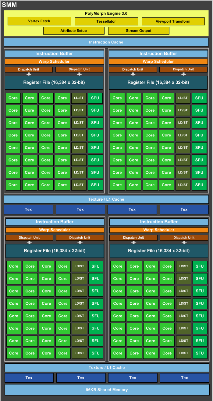
Take a peek at the SMM block (right) and Nvidia's realised it makes sense to split each SMM unit into, effectively, four sub-SM units. Each SMM now has four instruction buffers, register files, dispatch units and schedulers, compared to one larger version for Kepler, and doing so saves die space and power.
The 32 cores per sub-SM units is no accident. Unlike Kepler, these align perfectly to the way in which instructions are grouped into 32-thread warps and scheduled through the cores, again reducing obvious inefficiencies and increasing symmetry.
Just like the GTX 750 Ti, Nvidia has now combined the texture and L1 caches into one (in contrast to Kepler) and 96KB of per-SMM shared memory is now separate. Saving more die space, the ratio between cores and texture units now runs at 16:1, down from 12:1 on Kepler. This is why Maxwell has far fewer texturing units than Kepler.
There's more to it than just this alone, as well, as Nvidia removes a chunk of scheduling from the hardware and moves it over to software (GeForce driver), thus following Maxwell's mantra of saving space, reducing power and increasing efficiency.
Efficiency also means improved performance, as Maxwell's cores can be kept fuller and do more work than Kepler's, so merely looking at a shader-to-shader count is misleading. Nvidia claims that each Maxwell core, by dint of a wide range of improvements, offers 1.4x the performance of Kepler. Expressed roughly, 2,048 Maxwell cores are worth the same as GTX 780 Ti's 2,880 in Nvidia speak.
Yet it isn't all positive news. The way in which the SMM units are built means that each 128-core section contains four double-precision (DP) units. DP workloads execute at 1/32nd of the speed of SP, down from the 1/24th on Kepler. This fact is worth knowing if DP performance matters to you.
Putting Transistors In The Right Place
GeForce GTX 980 needs some more magic if it is to overhaul the bigger-die GTX 780(Ti). Good architecture design requires removing bottlenecks, so while texturing output has seen a chop, the render outputs (ROPs) - used to handle AA and masses of pixels - have been doubled, from 32 to 64. Maxwell puts transistors where newer games engines stall older GPUs. And appreciating these GPUs are likely to be run at high resolutions and image-quality settings, Nvidia equips both high-end Maxwell cards with a 4GB framebuffer.
Memory bandwidth is also a key component of overall performance. The on-paper specs, once again, make for decidedly average reading. GTX 980 has a 256-bit pathway connected to 7Gbps GDDR5 memory, which provides significantly lower bandwidth than, you guessed it, the GTX 780-series.
Nvidia uses a narrower bus to save on die space and power - can you see ongoing theme here? Getting around the obvious shortfall, particularly when memory is the bottleneck, GTX 980/970 quadruple the L2 cache, from 512KB to 2,048KB. More on-GPU cache costs in terms of transistors, of course, but more than pays its way by reducing the need to burn power when lighting up external RAM. Keeping work on the GPU speeds up performance, too.
Colour Me Up
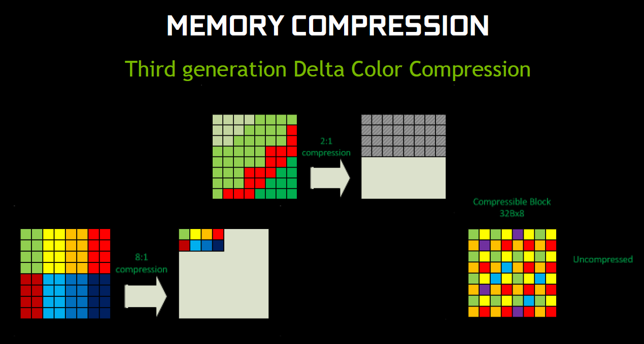
Having more on-chip cache only gets you so far; a 256-bit bus remains too narrow for a high-end card. All modern GPUs use some form of lossless compression to minimise the amount of data written out to memory, saving power and keeping performance high. Colour compression, as the name suggests, examines a frame and determines how many 4x2-pixel regions share the same colour. If they're exactly the same, they can be compressed on an 8:1 basis. If not, lower compression is considered.
 |
 |
Then there's delta colour compression which examines blocks of pixels and evaluates the difference between the two. Similar blocks have fewer differences and therefore less data needs to be written out across the bus. Algorithms manage how this compression/block similarity is processed.
Maxwell's larger cache and use of a third-generation delta colour-compression engine, which offers more means to compress the colour component of similar blocks, enables the new GPUs to reduce the amount of memory bandwidth required when compared to Kepler.
Nvidia says Maxwell can reduce the memory transactions by approximately 25 per cent. Putting it another way, memory would need to run at 9.3Gbps on a Kepler GPU to match the performance of the 7Gbps present on Maxwell. This is why the 256-bit memory bus isn't a huge concern on the GTX 980; real-word bandwidth is over 300GB/s, not the 224GB/s shown on the spec table.


