Volcanic potential
AMD launched a number of new graphics cards a couple of weeks back. But examining the details showed that the R9 280X, R9 270X, and R7 260X - the three headline GPUs - were largely rebrands of older technology. Countering a lack of genuine GPU advancement, AMD's attractive pricing makes the new cards reasonably compelling propositions.
The new, interesting GPU is the R9 290X, built using a brand-new die and designed for class-leading performance. Codenamed Hawaii and intent on a stare down with Nvidia's impressive GeForce GTX Titan and GTX 780 GPUs, today is reckoning day.
Radeon R9 290X
AMD has invested heavily in the GCN architecture powering all modern Radeons and, tellingly, the graphics in the Sony PlayStation 4 and Microsoft Xbox One consoles. In a nutshell, R9 290X taps into GCN a bigger way than previous Radeons, thus enabling higher performance via a wider, more parallel architecture. Let's take a peek at the Table of Doom™ and then dissect the GPU through analysis.
| GPU | Radeon R9 290X 4GB | Nvidia GeForce GTX Titan 6GB | Radeon R9 280X 3GB | Radeon R9 270X 2GB | Radeon R7 260X 2GB |
|---|---|---|---|---|---|
| Launch date | October 2013 | February 2013 | October 2013 | October 2013 | October 2013 |
| DX API | 11.2 | 11.1 | 11.2 | 11.2 | 11.2 |
| Process | 28nm | 28nm | 28nm | 28nm | 28nm |
| Transistors | 6.2bn | 7.1bn | 4.3bn | 2.8bn | 2.08bn |
| Approx Die Size | 438mm² | 551mm² | 352mm² | 212mm² | 160mm² |
| Processors | 2,816 | 2,688 | 2,048 | 1,280 | 896 |
| Texture Units | 176 | 224 | 128 | 80 | 56 |
| ROP Units | 64 | 48 | 32 | 32 | 16 |
| GPU Clock/Boost (MHz) | up to 1,000 | up to 876 | 1,000 | 1,050 | 1,100 |
| Shader Clock/Boost (MHz) | up to 1,000 | up to 876 | 1,000 | 1,050 | 1,100 |
| GFLOPS | up to 5,632 | up to 4,494 | 4,096 | 2,688 | 1,971 |
| Memory Clock (MHz) | 5,000 | 6,000 | 6,000 | 5,600 | 6,400 |
| Memory Bus (bits) | 512 | 384 | 384 | 256 | 128 |
| Max bandwidth (GB/s) | 320 | 288.4 | 288 | 179.2 | 102.4 |
| Power Connectors | 8+6-pin | 8+6-pin | 8+6-pin | 6+6-pin | 6-pin |
| TDP (watts) | 250 | 250 | 250 | 180 | 115 |
| GFLOPS per watt | 22.52 | 19.98 | 16.38 | 14.93 | 17.14 |
| Current price | $549 | $899 | $299 | $199 | $139 |
Architecture analysis - R9 290X
We've aligned the R9 290X up against the GeForce GTX Titan and R9 280X also from AMD. The new head honcho is essentially a scaled-up version of the R9 280X, which itself is based on a GPU that's nearly two years old.
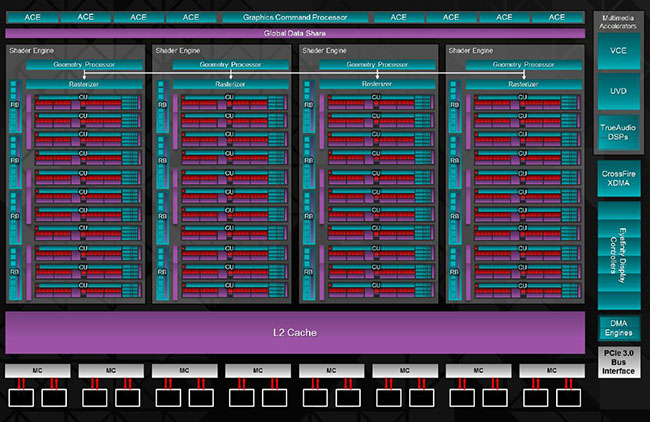
Here's a high-level overview of the 28nm-fabbed R9 290X. AMD's engineers have had ample time to understand the performance bottlenecks in the older Tahiti architecture and address them for this new Hawaii chip. As it is a fundamentally larger chip, R9 290X has a different mix of geometry, processor and backend setup.
Double down
Compared to previous generations, AMD has doubled the geometry processing at the top of the GPU. This processing takes basic data in, crunches geometry assembling, tessellation and vertex processing, and throws it over to the mass of compute units. Geometry performance is further improved, AMD says, by optimising local data storage and increasing off-chip buffering efficiency.
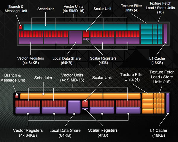
Moving on down, the central thrust of the chip is an increase in compute units, now numbering 44, up from 32 on the Tahiti-class Radeon HD 7970/R9 280X GPUs, but the actual composition of the CUs is the same.

R9 290X on the top and Radeon HD 7970 on the bottom. Both include four 16-wide SIMD vector blocks (the red ones, totalling 64 per CU), plus a scalar unit and registers in the middle, and a general, per-core scheduler at the top. You can see R9 290X's clock-for-clock processing ability is higher because it has more CUs and cores, though there are minor behind-the-scenes improvements that speed-up various common tasks. Bigger usually means better, so AMD boosts local storage cache from 768KB to 1MB, as well.
Raisin' the ROPs, and a clever trick with bandwidth
All this additional geometry and ALU horsepower is wasted if constricted by the ability of the GPU to process it, calculate the load for image-quality enhancements such as antialiasing, and then write this information out to the framebuffer before being delivered to your screen.
AMD doubles the render back-ends (ROPs) from eight to 16, and each can handle four colour and 16 Z/stencil operations per clock. Do the maths and the R9 290X can process 64 colour ROPs and 256 Z/stencils for every clock cycle, or double that of the previous Radeon champ, HD 7970.
Finishing this silicon jigsaw is a new memory controller that's suited to the R9 290X's greater grunt. AMD has pulled off the enviable trick of increasing the overall width to 512 bits, up from HD 7970's 384 bits, but, crucially, doing so whilst decreasing the required space by 20 per cent. This has been done by using space-saving PHYs that, unlike their Tahiti cousins, are not able to clock as high - you gain some space but lose on memory frequency potential. Smaller memory PHYs is one reason why the new chip, at 438mm², is only 25 per cent larger than the HD 7970/R9 280X.
A by-product of using a 512-bit bus is the ability to outfit the card with 4GB of equal-sized memory, which is the standard configuration for the R9 290X. This makes good sense for scenarios where you're running high resolutions and image-quality settings, especially with nascent 4K technology becoming more prevalent in the enthusiast space.
Frequencies, voltage and PowerTune
OK, so we know the R9 290X is faster/better than the previous generation because it has more of the ingredients that define modern-day gaming performance. The innate problem in engineering a bigger, wider GPU rests squarely with keeping power consumption in check. Literally scale up a R9 280X and power-draw will jump way beyond the accepted board limit of 250W.
AMD's solution in keeping maximum board power at around 250W is to use a sophisticated balance between GPU/memory frequencies, temperature and power. Alter one facet and you can manoeuvre the others to some degree. This is why the R9 290X is programmed with a native, guaranteed GPU speed of 800MHz, rising to 1,000MHz under optimum conditions - a take on Nvidia's GPU Boost, if you will. Following this energy-saving line of thinking, card memory is left at a conservative 5,000MHz, most likely due to using the smaller aforementioned memory PHYs.
By default the GPU is programmed to run with a toasty temperature target of 95°C. AMD's new PowerTune hardware uses a second-generation serial VID interface and VR controller, also seen on certain APUs, and they provide 255 voltage steps and 6.25mV granularity. This means the GPU's voltage and frequency can be controlled like never before. The card can be set to run at a very precise wattage, the fan-speed can be set to within tight parameters, and ideal temperature to within a single degree. The purpose is to extract the most performance for a given power and thermal budget.
You set the desired parameters - wattage, temperature, etc. - and the GPU ramps up in accordance. There's no guarantee that it will hit 1,000MHz every time, but loosen off the shackles, at the expense of power, noise and temp, and the R9 290X will run faster. We'll show you just how this correlates to real-world gaming in the benchmarking section.
More integration than ever before
AMD removes the need for external CrossFire connectors by integrating a hardware DMA engine within the silicon. This compositing block enables direct access between the GPUs' displays through the PCIe bus. R9 290X is plumbed with six display connectors, bifurcated between two dual-link DVI, HDMI, and a single DisplayPort that supports a trio of multi-stream transport-attached displays.
Price
There has been plenty of conjecture surrounding the R9 290X's price. AMD has come in at $549, thus heavily undercutting the $899 GeForce GTX Titan and being $100 cheaper than the GeForce GTX 780. This is a huge deal should the card perform to the levels intimated by the specifications.
Summary
AMD's Radeon R9 290X is the biggest GPU ever produced by the company. Weighing in at 6.2bn transistors and ostensibly a scaled-up version of the Radeon HD 7970/R9 280X, albeit with a number of improvements. Drawing a very tenuous analogy, R9 290X is akin to adding an extra lane and traffic-management system to the Radeon HD 7970/280X three-lane motorway. The end result is a wider road that's primed to keep traffic (read instructions) moving along nice and efficiently.
So massively wide at the top and the bottom, AMD is bullish about the range-topping GPU's potential for running games at a 4K resolution. But before we go that far, let's use this review to examine if it can handle Nvidia's GeForce GTX Titan and GTX 780 GPUs. The on-paper specifications suggest that AMD should have the upper hand - the R9 290X has more compute and memory bandwidth on tap - but Nvidia GPUs tend to punch above their weight in games.


