


Snippety-snip
NVIDIA is on something of a roll at the moment. While AMD will doubtless argue to the contrary, NVIDIA has the best single- and dual-GPU graphics cards on the market. As nice as the GeForce GTX 680 and GTX 690 patently are, the entry price into this lofty club is a cool £400, rising to almost £900 for the best of the best.
The green team needs to cascade its Kepler-based GeForce goodness to lower price points that characterise the mass market. The first step into this much-needed filling out comes by way of another enthusiast-class GPU, the GeForce GTX 670.
GPU manufacturers adopt a common tactic of launching with the best-possible single-GPU card first and then, a short while later, bring in a slightly cheaper, less powerful version. Whether you care for the pragmatics of silicon manufacturing or not, this second-rung offering usually takes in those GPUs that don't quite make the A-grade, which in this case is the GTX 680. Manufacturing partner TSMC determines which wafers lie on the low side of the yield curve, for whatever reason, and NVIDIA repurposes them as the slightly slower parts. That, in a nutshell, is how the GeForce GTX 670 comes into existence.
NVIDIA, therefore, has to make a trade-off between performance and silicon yield. It wants to make the most money out of costly GPU wafers but doesn't want to hamstring this second-rung GPU too much, considering that it'll go up against AMD's robust Radeon HD 7970 and HD 7950 GPUs, so let's see just what kind of machinations are afoot with the Trusty Table™.
| GPU | GeForce GTX 680 (2,048MB) |
GeForce GTX 670 (2,048MB) |
GeForce GTX 580 (1,536MB) |
Radeon HD 7970 (3,072MB) |
Radeon HD 7950 (3,072MB) |
|---|---|---|---|---|---|
| DX API | 11.1 | 11.1 | 11 | 11.1 | 11.1 |
| Process | 28nm | 28nm | 40nm | 28nm | 28nm |
| Transistors | 3.54bn | 3.54bn | 3.0bn | 4.3bn | 4.3bn |
| Die Size | 294mm² | 294mm² | 520mm² | 352mm² | 352mm² |
| Processors | 1,536 | 1,344 | 512 | 2,048 | 1,792 |
| Texture Units | 128 | 112 | 64 | 128 | 112 |
| ROP Units | 32 | 32 | 48 | 32 | 32 |
| GPU Clock (MHz) | 1,006 (1,058) | 915 (980) | 772 | 925 | 800 |
| Shader Clock (MHz) | 1,006 (1,058) | 915 (980) | 1,544 | 925 | 800 |
| GFLOPS | 3,090 | 2,459 | 1,581 | 3,789 | 2,867 |
| Memory Clock (MHz) | 6,008 | 6,008 | 4,008 | 5,500 | 5,000 |
| Memory Bus (bits) | 256 | 256 | 384 | 384 | 384 |
| Max bandwidth (GB/s) | 192.3 | 192.3 | 192.4 | 264 | 240 |
| Power Connectors | 6+6 | 6+6 | 8+6 | 8+6 | 6+6 |
| TDP (watts) | 195 | 170 | 244 | 250 | 200 |
| GFLOPS per watt | 15.84 | 14.46 | 6.32 | 15.15 | 14.34 |
| Release MSRP | $499 | $399 | $499 | $549 | $449 |
We have five of the best GPUs in the graphics-card business lined up against one another: three from NVIDIA and two from AMD. The wonders of a 28nm process mean that while the GTX 670/680 fit in more transistors - read performance - than last-generation GTX 580, their die size is over 40 per cent smaller. This is a good thing for NVIDIA's bottom line, assuming GTX 670/680 GPUs are yielding reasonably well.
GeForce GTX 670 vs. GTX 680
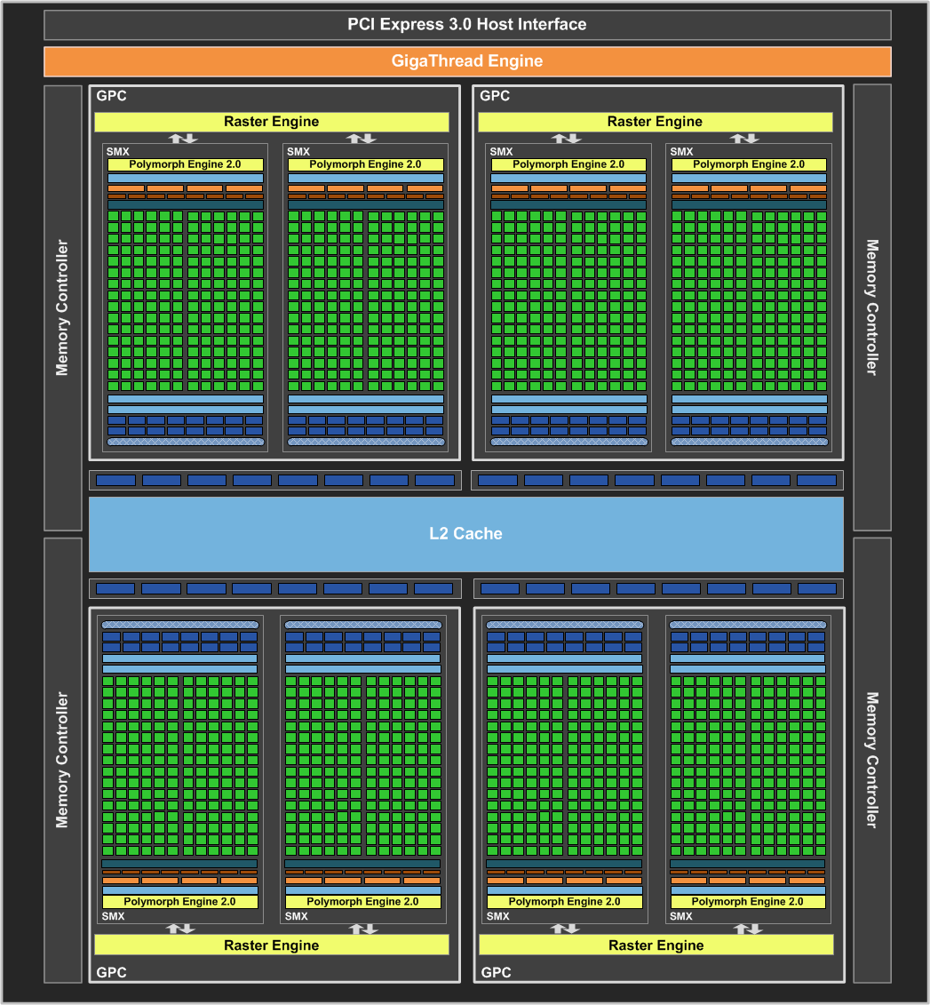
The real comparison, however, is between the two premium NVIDIA cards. Leading on from what we discussed above, GTX 670 shares the same die as GTX 680, though the performance compromise comes by way of fewer shaders and lower frequencies. GTX 670 misses out on one of the GTX 680's SMX units - down to seven from eight - and decreases the default core/shader frequency to 915MHz, from 1,006MHz. And that's it; no other obvious performance concessions are apparent.
One SMX unit is home to 192 cores, 32 special-function units, 32 load/stores, 16 texture-units, one setup engine (PolyMorph 2.0), and four warp schedulers that can each dole out two 32-thread instructions per clock. Get past the geek-speak and this means, overall, GTX 670 has 1,344 cores and 112 texture units, or about 12 per cent less than GTX 680.
The base clock is set to 915MHz though, on average, it goes up to 980MHz when evaluated across a wide range of games. Fewer cores and a lower core clock translate to approximately 20 per cent less computational and texturing throughput but NVIDIA gives it a helping hand by keeping the memory speed at a GTX 680-matching 6,008MHz. So, really, you've got a marginally pared-down top end and the same backend as GTX 680.
It's pretty easy to hypothesise GTX 670's performance; it should benchmark at around 90 per cent of a full-fat GTX 680. One obvious benefit of removing or deactivating a few parts of the architecture is lower power-draw. GTX 680 is hardly a hot, thirsty beastie, granted, but GTX 670 drops the maximum TDP down by 25W, to 170W: nice.
We expect the GTX 670 to cost $399 (£330) for stock-clocked models, rising to £350-plus for partner-overclocked editions from the usual suspects.


