


Fermi for everyone
Mainstream machinationsGraphics giant NVIDIA is unveiling its latest GPUs today. Based around the Fermi architecture first brought to bear earlier this year, the company is now looking to solidify the mid-range appeal of the $175 GeForce GTX 460 cards by debuting new graphics processors at a lower price point.
The GeForce GTS 450 is the GPU that NVIDIA hopes will persuade purchasers to shy away from AMD's mid-range Radeons - HD 5670, 5750, and 5770 - and spend their cash on the newest GeForce hardware. NVIDIA is squarely targeting the $129 Radeon HD 5750 with this new GPU, and this review will determine if NVIDIA's managed to balance snips in architecture and performance with the keener price.
Architectural derivations - half a perfect GF 104
GeForce GTS 450, also known as GF106 in architecture terms, is a design that's largely based upon GTX 460 (GF104), so let's start with the latter's block diagram and work our way towards the all-new GF106.
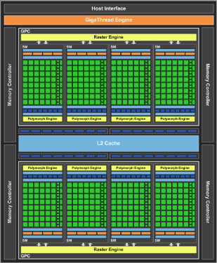 GF104
GF104What you're looking at is a full-fat GF104 block diagram. Composed of eight Streaming Multiprocessors - blocks of shader units - that house 48 CUDA cores each, the design allows for a total of 384 shaders. These are backed up by 64 texture units - eight per SM - 512KB of GPU-wide L2 cache, 32 ROPs and a 256-bit memory interface to GDDR5 memory.
The GeForce GTX 460 GPU, available in both 768MB and 1,024MB flavours, uses seven of the eight SMs, presumably currently hamstrung due to yield concerns. The 1,024MB card is equipped with a full complement of supporting logic, while the 768MB GPU's design is such that it provides 24 ROPs and a 192-bit memory interface. Both, however, are clocked in at the same speeds.
NVIDIA has taken a good look at the full-architecture GF104 die and decided that the best method in reducing manufacturing costs while still providing class-leading performance in the mainstream market is to cleave the GF104 die into two.
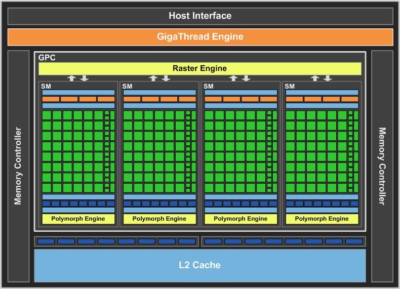 GF106 (kind of*)
Et voila, monsieur, 'alf a full-fat GF104. The new GPU is composed of one GPC, meaning that it's home to 192 CUDA cores (shaders), 32 texture units, 16 ROPs, 256KB L2 cache, and a 128-bit memory interface to 1,024MB of GDDR5 memory. GeForce GTS 450, then, can be considered to be slightly more than one-half a retail GeForce GTX 460 1,024MB card.
*Interestingly, NVIDIA GF106's full functionality is realised in a design that has three memory-controller partitions and three associated ROPs, leading to a 192-bit interface and 24 ROPs in total. NVIDIA, however, has made no indication of bringing this particular design to market, so all shipping GF106 parts will have two sets of eight ROPs and a 128-bit interface.
The economics of manufacturing dictate that smaller dies are cheaper to produce and, ceteris paribus, will have higher yields. NVIDIA is literally banking on this fact, as the GF106 weighs in at 1.17bn transistors, compared to GF104's 1.95bn.
Speeds and feeds
An aggressive chop in architecture means that NVIDIA needs to keep GPU frequencies at high levels in order to compete with the mid-range Radeons. To this end, the GeForce GTS 450 1,024MB is rated at 783MHz core clock, 1,566MHz shaders, and 3,608MHz memory. Compare this with a 675MHz core and 3,600MHz memory clocks on the GTX 460.
The modular nature of the Fermi architecture and incumbent GTX 460 design largely dictates how the newest GPU of the Fermi clan, GTS 450, is going to look and perform. There are no real surprises here, but the recent price reduction of GTX 460 cards - a 768MB GPU currently retails from £120 - intimates that NVIDIA's price positioning is vital for the nascent success of the GTS 450. Let's now stack it up against its most-immediate competition.


