


More tech: texturing, ROPs and memory bandwidth
Texture performance and speed see a bump, too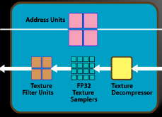
Changing the internal layout some more from RV670, the 10 cores, containing 80 SPs, are now coupled to a specific texturing unit that has four texture-address processors and four FP32-type texture-filter units. That's 40 of each, thinking of it in a GPU-wide sense, and, as such, is also 250 per cent higher than RV670's 16, keeping the arithmetic-to-texture ratio intact.
Why 4:1 still? ATI's engineers reckon that whilst certain games hugely favour the shader units, citing examples such as Crysis that can have an 8:1 ALU-to-texture ratio, others still use far more conservative ratios, even down to 1:1.
The 10-core-toting GPU, then, can address and bilinear-filter at 40 pixels per clock cycle. Funnily enough, that's 2.5x RV670's. Seeing a theme here? FP16, however, is now filtered at half speed - 20ppc. Lots of bilinear filtering and reasonable FP16 filtering, assuming decent core clocks. Trilinear and anisotropic filtering can also be run on all textures, irrespective of their precision, as well.
Much like the SPs, the texture units are now significantly smaller than RV670's - some 70 per cent smaller, according to ATI. Again, we wonder what extra baggage RV670's was carrying that can suddenly be jettisoned in just over six months? Perhaps the HD 48x0's inability to FP16-filter at full speed saved some space?
Looking a little wider, the texture units are connected to L1 texture cache, just like RV670, but, now, the bigger L2 cache, whilst still in touch with L1, is further connected, via a ringbus-style controller, to the memory channels.
Each SIMD has its own L1 TC, whose contents can be different from the other cores' L1 TCs, and goes against the fully-shared approach on RV670. L2 cache is present to ensure that various cores' SIMDs don't try to grab the same texels, meaning duplicate memory requests, when their L1 TCs have the same data.
Knowing that the L2 TCs are connected to the memory, there's 115GiB/s from memory to L2 TCs, some 384GiB/s between L2 and L1 TCs, and 500GiB/s from L1 TCs to the texture filters. Phew!
The vertex cache is now independent of the texture caches, rather than the bolt-on process with HD 3870. The handy crossbar switch connects the vertex cache with the texture caches.
Only 16 ROPs?
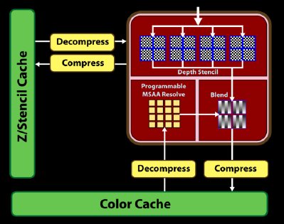
We've come right down to the raster back-ends, or ROPs. Keeping with the theme of smaller is better, the new ROPs were designed by the team behind the X1900 series.
RV770 carries over the previous generation's four ROPs and each can process four pixels per clock, or 16 in total. Based on mid-range core speeds, pixel fillrate won't be hugely impressive, then. But that's doing RV770 a little disservice, because it ignores improvements made to the ROPs with respect to anti-aliasing, where pixel throughput is eaten up.
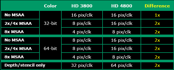
16ppc is still the count when no AA is taken into account but, according to ATI, the processing ability of RV770 is significantly better when multisampled antialiasing is introduced, up to 2x improvement in most cases. Pragmatically, this should lead to a smaller hit when invoking AA at high resolutions, and we'll put this to the performance test in our benchmarks.
On the flip-side, however, RV770 may well be constricted when rendering without additional image enhancement, because the back-end, limited to 16ppc, can't fully utilise the shading and texturing power on offer, inferring that HD 4850's performance will be closer to HD 3870's than the specifications otherwise suggest.
Z throughput has been doubled from RV670, from 32 to 64ppc, in both AA and non-AA cases. It's important because Z (depth buffer) is used for various shadowing and lighting performance.
Antialiasing levels remain the same, at up-to 12x CFAA (Custom Filter AA) in single-GPU mode and up-to 24x in CrossFire. However, higher-quality, but slower, box filtering, for AA resolve, has now been brought back, too.
ATI reckons that overall compression and memory bandwidth utilisation has been improved to the extent that running 8x AA isn't markedly slower than 4x AA.
Memory bandwidth
ATI has retained the 256-bit memory interface that's found on the HD 3800-series of GPUs, and down from the die-space-taking and power-consuming 512-bit on the extant Radeon HD 2900 XT.
Specifically, four pairs of 32-bit channels are combined to offer frame-buffer-to-GPU bandwidth.
The GPU's memory controllers can either interface with tried-and-trusted GDDR3 modules, used for the Radeon HD 4850, or with all-new GDDR5, debuting on the Radeon HD 4870. GDDR5, now produced in relative volume by the likes Qimonda, provides inherently faster speeds by using two concurrent links to double transfers compared to the incumbent solutions' - GDDR3, GDDR4, and GDDR5 - one.
Interestingly, the architectural design to run with a 256-bit bus was made well before the availability of GDDR5 had been known. Had its introduction been delayed by, say, six months, ATI would have found itself in an embarrassing situation of a bandwidth-limited Radeon HD 4870.
Still, we reckon that the BOM (bill of materials) cost for GDDR5 is significantly higher than GDDR3 and that it makes up a fairly large proportion of the HD 4870's etail cost. Cutting-edge technology is rarely cheap.
Having high memory clockspeeds negates the disadvantage that a 256-bit controller imposes, and ATI will debut Radeon HD 4870 with memory running at an effective 3.6GHz - yup, 3.6GHz.
Knowing that the interface is 256-bit, made up of eight 32-bit channels, ATI (and its partners) need to use 'only' eight DRAM modules rather than the 16 mandated if running a 512-bit path to the ROPs.
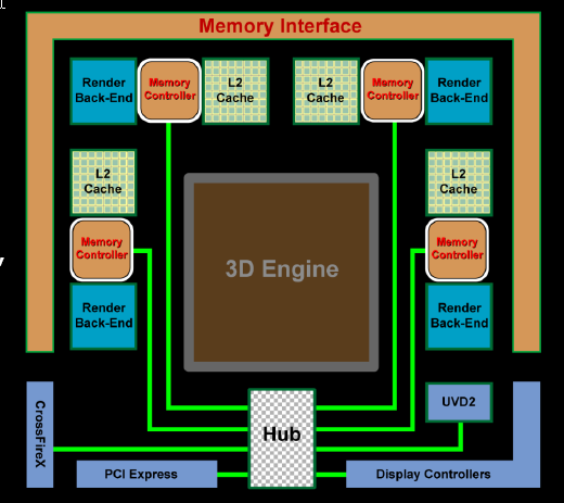
ATI reckons that the new memory-controller architecture and pairs of channels are now better distributed around the chip, closer to the bandwidth-consuming ROPs and caches that they primarily serve. They're situated such that they don't need to go on the ringbus memory controller, wasting time, anywhere near as much as, say, Radeon HD 3870's do. The bandwidth has also been internally doubled from controller to client - be it ROP or L2 cache. ATI claims that such an approach raises peak bandwidth utilisation to around 95 per cent of what's theoretically available, compared to 85 per cent for RV670.
A separate hub then connects low-bandwidth output and dishes it to the usual receptors: PCI-Express 2.0 for the system, display controllers for output, and CrossFireX for multi-GPU rendering.
Other tweaks
In cleaning up RV670's architecture, ATI reckons it has improved the geometry-shader performance by enhancing the geometry-amplification stage - where more generated data is kept on-chip and re-used without having to pop on over to main memory.
Multimedia enhancements
There's now an upgraded UVD block, called UVD 2, that hardware-accelerates the decoding of two video streams running concurrently. There are only few instances where we can see this being useful - picture-in-picture commentary, for example. We note that NVIDIA introduced this feature at the back end of last year.
Following the same theme - a la NVIDIA - there's now provision for dynamic (card-based) contrast adjustment. Further, the UVD 2 block contains new algorithms to better upscale DVD content to high-definition status.
ATI's Radeon HD cards have benefited from on-GPU HDMI support from the get-go. The elegant approach sees the motherboard's audio routed through the GPU and out of the back, through either a native HDMI or DVI-to-HDMI converter.
Previous generations utilised HDMI v1.2. This has now been upgraded to most of the HDMI v1.3 feature-set, including 7.1-channel audio (on v1.2, too) and Dolby TrueHD and DTS-HD formats. What's more, 8-channel sound can be sent through in an uncompressed format - well, LPCM, actually - nice for HTPC users.
Much like NVIDIA, ATI will be releasing patched software that uses the GPU's stream processors to transcode high-definition video into other formats. The CPU-to-GPU speed-up, from dual-core Intel CPU (E8500) to HD 4870, is reckoned to be in the order of 19x for a one-hour 1080p video. We expect to see it implemented in CyberLink's PowerDirector v7 software this month, which also supports simultaenous encoding of a number of HD videos, too.
CrossFireX
ATI's multi-GPU technology, CrossFireX, is supported by the HD 4800-series of GPUs. You have the option of running up to four boards for increased frame-rates, but scaling above two produces significantly diminishing returns.
Whilst technically you can couple boards from different generations - Radeon HD 3870 and HD 4850 - CrossFireX only works well with cards from one family. HD 4850 and 4870 can be combined, of course, but the resulting output will be based on the slowest card in the outfit.
Drivers
RV770 will ship with Catalyst 8.6 drivers for Windows XP and Vista .We're glad to see that ATI will have zero-day support for Linux x86 and x86-64 platforms, too.
Make it simple, stupid!
There's a lot to take in here. The RV770 architecture has been significantly streamlined in the transition between the HD 4000- and HD 3000-series. That streamlining, which consists of making units smaller and generally more efficient, has led to ATI packing the 260mm chip with fundamentally higher stream processors and texturing units: the two blocks required for fast processing.
ATI's been keen to pack as much power into a small a die space as possible, where each die's size directly reflects upon the cost structure, hence the continued use of a 256-bit memory controller. Doing so inexorably leads to bandwidth implications that are partially offset by using the latest technology, GDDR5.
Architecturally, RV770 is a lean, mean design that won't win the absolute performance awards: NVIDIA's double-sized GeForce GTX 280 has greater overall horsepower. Rather, Radeon HD 4850 and 4870 should beat present Radeon HD 3870/50 to a performance pulp, yet with a die size which is only 35 per cent bigger.
Let's talk numbers now....


