


All the technical bits
Lots of concurrent threads are good, of course, but they only tell part
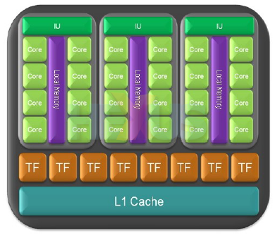
of the story. Each of the GTX 280's 10 clusters has what NVIDIA terms a
dual-quad texturing unit, and you see that represented by the eight
brown TFs in the cluster picture.
Filter me, baby
As with the GeForce 9-series, each GTX 280 cluster unit can address and filter eight bilinear pixels per clock - based on eight-bit integer, INT8 - or four 16-bit floating-point pixels (useful for HDR), meaning half speed.
ATI's Radeon HD 3870 can address and filter FP16 pixels at full speed,
however, but its filtering is compromised by a lack of texture-units.
Going back a generation, GeForce 8800 GTX, on each of its eight
clusters, was also able to texture-filter eight pixels per clock - just
like GeForce 9 and GTX 280 - but could only texture-address and
bilinear-filter (INT8) four per clock. Each unit could also handle four
FP16s. Kind of complicated, huh?
Bottom line: the matched addressing and texturing capabilities are
carried over from the 9-series GPUs. But we'd have been happier seeing FP16
texturing being filtered at full speed.
Overall, though, NVIDIA wins the FP16 pixel-filtering battle. GTX 280
can do 40ppc, 9800 GTX 32ppc and ATI's Radeon HD 3870 a total of 16 -
the same as its texture-unit count.
Adding it all up, GeForce GTX 280 beats out GeForce 9's filtering by
having more clusters - 10 versus eight - meaning bilinear filtering of 80
pixels per clock compared to 64 per clock.
NVIDIA needs to strike a decent balance between the texturing and
shading ability of the GPU and, when comparing against previous unified
architectures, the provision of more shaders to texture units is
probably the way to go - 24 per cluster versus 16.
The missing MUL
There was a little controversy over how the GeForce 8-series and 9-series
GPUs aggregated floating-point power.
Using the basic maths building-blocks of MADD (multiply-add) and MULs (multiply), the GPUs were reckoned to be able to dual-issue both a MADD and MUL at the same time, meaning three FLOPS (MADD counts as two) per stream processor, per clock cycle.
It transpired that the MUL part of the deal that was
handled by another part of the architecture, so, accurately, the GPU could process
three FLOPS per cycle when in full-blown dual-issue mode.
Why are we boring you with this, you might ask? Calculating and being
able to access close-to-peak FLOPS throughput is important for gaming and, rather more so, for GPGPU tasks.
FLOPS throughput will
probably be hindered by other factors such as memory bandwidth - which
we'll come to - and memory access, but bigger is better.
GeForce GTX 280's 240 stream processors can still only process two
FLOPS - multiply and add (MUL and ADD = MADD) - per clock cycle but a
'special-function' unit, like that on the older architectures, located
within the streaming multiprocessors,
can perform the additional MUL. That's a roundabout way of saying that
the architecture can issue three FLOPS per clock cycle, albeit not all
purely from the SPs.
NVIDIA reckons it has improved the dual-issue nature of the GTX
200-series with some behind-the-scenes tweaking. Running 3DMark Vantage
may help shed some light on this.
What else is there to say
about SPs, SMs and whatnot?
Each SM has its own 16KiB of local memory and can
share the contents of its memory with the other two SMs in the cluster
without having to run to main system memory and back again. NVIDIA
reckons that this ensures greater efficiency by reducing latency - something we'll be putting to the test.
Just like G80, each cluster has its own L1 cache which connects to the
ROPs - where all the back-end work takes place, including antialiasing -
and then out to main card memory.
ROPs
GTX 280 carries eight ROPs (raster operators) - seen in
red and blue - that can each process four pixels per clock. GeForce 8-series
and 9-series GPUs have six such partitions, again capable of four ppc.
The new SKU, however, can also blend at 32 pixels per clock, whereas G80
needed to split a blender between two ROPs, leading to a 24 ROP (6x4)
and 12-blend count. In short, greater than 33 per cent more ROPs and better than 3x the blending, at equal clock speeds.
Memory
Coming down further, each ROP has access to a little L2
cache and a 64-bit connection to main memory. Combining the 64-bit
pathways with the eight channels, GTX 280 supports a 512-bit interface - twice that of GeForce 9800 GTX and higher than the 384-bit pushed with
the original G80s. Having bags of fast memory is always good for the
ROPs, especially when loaded with resolution and copious amounts of
filtering.
GeForce GTX 280 is equipped with a 1GiB frame-buffer, though NVIDIA opted to
go with GDDR3 DRAMs to keep costs relatively in check.
Other new bits and pieces
ATI introduced double-precision (64-bit) floating-point
compliance with its Radeon HD 3000-series and NVIDIA's
GTX 200-series supports it, too, via what's termed a fused-MADD. The ability is useful for
the GPGPU environment where calculation accuracy is absolutely
paramount.
Double-precision calculation, of course, takes away throughput - you
can have one or the other at the same time. GTX 280 can operate with 30
double-precision processors - or one-eighth speed - working in a
concurrent manner.
It's likely, though, that 64-bit floating-point computing will remain the domain of
high-end CPUs until NVIDIA or ATI launches a specific GPU for this
purpose.
Geometry shading, which is part of the DX10 specification, and Stream Out - a sub-set of the geometry shader - have both been greatly improved,
according to NVIDIA.
Stream Out is handy when you want to continually re-use previously-generated data without having to
re-render it, saving bandwidth and time.
NVIDIA has also increased what's termed the register files. Put simply,
they're storage spaces on the streaming multiprocessors that hold the
shaders, ready for execution. Super-long shaders caused the G80 to fill
its register space, thus requiring main memory to lend a hand. Bottom
line - larger register files mean more on-chip action and, potentially,
higher performance.
There's been a general cleaning-up of the architecture, ranging from greater efficiency at memory accesses to better compression and Z-cull performance - where you occlude pixels that won't be shown - at higher resolutions.


