Tick, followed Tock, followed Tick...
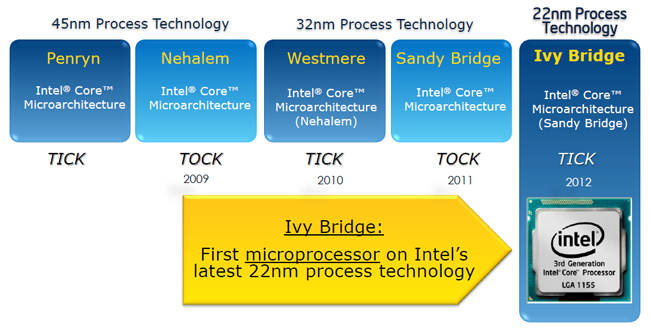
If there's one thing we should know about Intel processor technology, it's that it progresses like clockwork. We see a new fabrication process every two years (45nm in 2008, 32nm in 2010, 22nm in 2012, and so on) accompanied by a relentless Tick Tock release schedule. For those unfamiliar with Intel parlance, let's expand on the latter.
Roughly every 12 months, Intel launches a new CPU architecture on what the manufacturer calls a 'Tick Tock' sequence. Generally speaking, the Tock refers to major architecture revamp, while the Tick insinuates a minor architecture refresh coupled with a shrink in manufacturing process.

Going back through the history books, Nehalem provided a major Tock to Penryn's Tick, Westmere ushered in the 32nm era, Sandy Bridge provided one of the most memorable Tocks of all time, and today, a little something called Ivy Bridge arrives to keep Intel innovation Ticking over for another year.
Using recent history as a guideline, we know that Intel attempts to launch something revolutionary on a two year cadence, and then fills the void in between by introducing a product that makes the previous best that little bit better. Applying that formula to what's new and upcoming tells us that Ivy Bridge is Sandy Bridge with sugar on top, and Haswell - a codename you'll be hearing more of in 2013 - will be formed from an entirely new microarchitecture recipe.
The Tick, then, is the Intel equivalent to Football's European Championship - you know it's going to be good, and you might even buy a ticket, yet it's the World Cup that follows that's really whetting your appetite. But your interest in Intel's 2012 Tick shouldn't wane based on terminology alone, as there's more to Ivy Bridge than meets the eye.
Introducing the 22nm Tri-Gate transistor
"The number of transistors incorporated in a chip will approximately double every 24 months."
— Gordon Moore, Intel Co-Founder
Ivy Bridge's first claim to fame is that it ushers in Intel's 22nm Tri-Gate transistor technology. This isn't something that's going to answer the question that troubles the masses - should I buy Core i3, i5 or i7 - but it's an important behind-the-scenes development and one that deserves a mention.
First, a little primer. Transistors are the key active components in today's processors and their miniaturisation is regularly cited as the driving force behind modern electronic devices. Making transistors smaller allows for a greater number to be incorporated in a chip, and as Intel co-founder Gordon Moore famously predicted; the number of transistors in a chip will approximately double every 24 months.
The increase in the number of incorporated transistors is tightly linked with performance, but keeping up with Moore's Law is an engineering challenge. Die shrinks have been, and continue to be, a contributing factor to Moore's Law, but in its move to 22nm Intel is also introducing Tri-Gate technology that improves performance and efficiency.

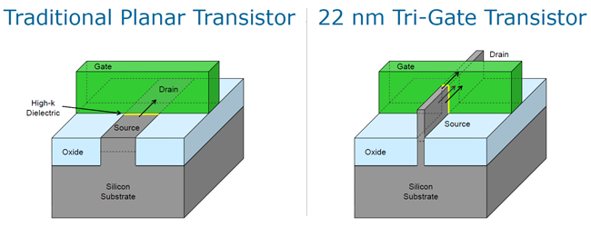
Here's how it works. An Intel transistor creates a stream of electrons channelled through a high-k metal gate that controls the flow. When the gate in on, free electrons are attracted to the surface allowing current to flow. When the gate is off, the conducting surface is depleted of free electrons resulting in little-to-no flow.
The idea is to have as much current flowing as possible when the gate is on, as little flow as possible when the gate is off, and to switch between the two states as quickly as possible. Sounds easy enough, but remember that a traditional 32nm planar (2D) transistor is so small that more than 60 million of them would fit onto the head of a pin, and as transistors get smaller, it becomes more difficult to control leakage (where electrons continue to slip through the gate).
And that's where Tri-Gate (3D) transistors come in. As pictured above right, a Tri-Gate transistor features conducting channels on three sides of a vertical fin structure. This provides a larger surface area for current to flow when the gate is on, resulting in greater performance at a lower operating voltage, with the option to add multiple fins, and reduced leakage as a result of the gate squeezing out free electrons from all three sides.
According to Intel, this implementation provides an 18 per cent performance increase in gate switching over the previous 32nm process when operating at 1V. And the improvement has been a long time coming - the Tri-Gate transistor has been in development for the best part of 10 years and given the improvements discussed above, Intel will now be using this technology for all future CPUs.
Enabling efficiency
We've established that Intel's 22nm Tri-Gate transistor technology is a good thing, and that's a fact that becomes more apparent when you examine the product.
Take, for example, the previous-generation Core i7-2700K. The range-topping 32nm Sandy Bridge processor features four physical cores as well as integrated graphics, built into a 212mm² die that utilises 1.16 billion transistors. It's an impressive chip, but the 22nm Ivy Bridge equivalent - the Core i7-3770K - is far more advanced.

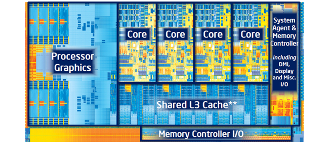
Here's the overview of the Ivy Bridge die. It looks seemingly-identical to the incumbent Sandy Bridge; it features the same numbers of IA cores alongside integrated graphics and a shared cache, but the shrink in fabrication process has allowed Intel to package the components in a 160mm² die carrying a meaty 1.40 billion transistors.
That's a near-25 per cent reduction in die size coupled with a 20 per cent increase in transistor count. Both the aforementioned chips run at the same core clock speeds - 3.5GHz with a maximum Turbo frequency of 3.9GHz - but the TDP is reduced from 95W for the 32nm Sandy Bridge part, to 77W for the 22nm Ivy Bridge successor. All the raw speed, but the chip as a whole is 19 per cent more efficient.
Improving efficiency is very much the name of the game, but Intel has bundled in a sprinkling of other upgrades, too.


