Goodbye, Phenom, hello, FX
K10, a fond farewell
AMD has pulled significant mileage out of its Athlon and Phenom CPUs. Tracing the lineage all the way back to 2003 with the release of the Athlon 64, architecture modifications - K8 to K10 - die shrinks, socket longevity, and across-the-board price-cutting means that, eight years on, the company's six-core Phenom II chips remain solid choices for a mainstream build.
Meanwhile, competitor Intel has launched a raft of new technologies and architectures in the same eight years, culminating with the impressive second-generation Core chips released in January 2011. To draw a tenuous boxing analogy, AMD's Phenom II is a boxer whose past his prime, and while price-cutting can mask a foible or two, there's not a whole lot of time left until he hits the canvas and simply fails to get up.
AMD's not stood still while Intel's been 'tick-tocking' its way to ever-more efficient, leaner CPU-and-GPU architectures. It's brought its own Fusion to play with the all-new desktop Llano, packaging a healthy dollop of GPU performance with an adequate CPU. Now ready to take the fight to Intel is a range of new mainstream CPUs that are designed to replace Phenom II. Enter the Bulldozer family.
FX, the pound-for-pound champion?
Making a clean break from the K10-derived Phenom II architecture, everything about Bulldozer is new. There's a new fabrication process, general architecture, ISA support, cache setup, power-delivery system, and branding: phew! Let's get under the skin of Bulldozer by examining each in turn.
32nm production
Following on from the process adopted for the CPU-and-GPU Llano, AMD is using 32nm Silicon-On-Insulator High-K Metal Gate fabrication from GLOBALFOUNDRIES. 32nm is a must in late-2011, and it enables AMD to squeeze in more transistors than the 45nm process used for Phenom II.
But GloFo has endured well-documented problems in ensuring a steady supply of Llano chips. Just how this will translate to Bulldozer yields is a closely-guarded secret for now, though AMD's PR machine has responded by stating there will be 'adequate supply' in the channel, whatever that really means. AMD absolutely needs to support its partners and the channel when faced with abundance of Core chips flying out of Intel's fabs.
Architecture - a new beginning
Here's where it gets interesting. AMD acutely understands that any new architecture needs to scale in terms of cores, power and performance, enabling it to fit into laptops, desktop machines and servers. And it's in response to this required scaling that, literally, a modular architecture has been designed.

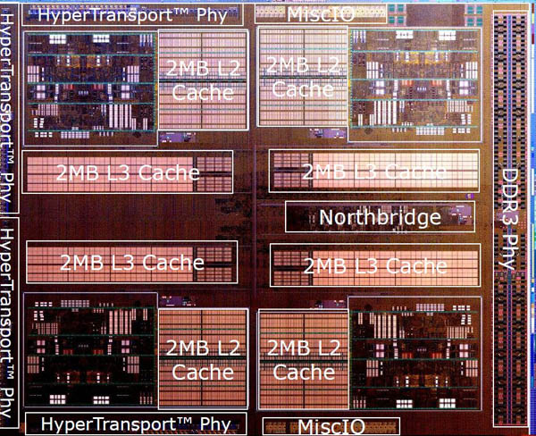
Here's Bulldozer as seen from a high-level overview. A quick glance shows there to be four execution cores surrounded by lots of cache - 16MB, in fact. With dual-channel DDR3 memory interfacing with the on-chip northbridge, L3 cache, and four HyperTransport links out to the rest of the system, there doesn't seem to be a whole lot new here. It won't escape your attention that in no portion of the picture is there reference to integrated graphics: Bulldozer is a pure CPU.
But first glances can be misleading. You see, while there's no provision for integrated graphics, there are eight CPU cores present here, but each core doesn't quite fit into the fully-independent mould established by processors of yore. There be some explainin' afoot, so let's zoom into one-quarter of the chip.

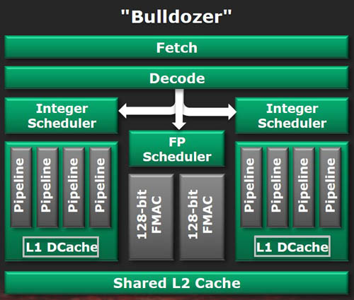
Here's a simple overview of what's going in one module. It's important to understand that Bulldozer is built through modules, where an eight-core chip has four modules, a six-core chip has three active modules, and a four-core, well, two: you get the idea. Putting it into perspective, a four-module, eight-core chip weighs in with nearly two-billion transistors (ahem, 1.2bn, after AMD acknowledges counting mistake) and has a die size in the region of 315mm². Interestingly, this is the same size as a six-core Phenom II die, albeit it's manufactured on the larger 45nm process. Intel, however, manages to pack four cores, eight threads, and integrated graphics (Core i7 2600K) into a significantly smaller die.
AMD doesn't have two fully-independent cores per module, but neither is it as integrated as, say, the hyper-threading cores found on Intel's latest chips, where resources are well and truly shared between processors. The reason for this core mishmash rests with balancing die size - and, therefore, manufacturing cost - against core throughput. In a world that cared little for economic cost, AMD would engineer Bulldozer with eight independent cores, along with all the necessary per-core silicon that entails.
Taking Bulldozer for what it is, let's assume two threads are moving through this module, to be processed on each core. They have to share the setup stage - fetch, decode - as well as the (much larger) floating-point scheduler, and, labouring a point that's important to understand, this would not happen on truly separate cores. However, the decode stage has been boosted to four instructions per clock cycle, up from three on Phenom II (albeit per core), and, through a technique called branch fusion, Bulldozer can actually make the decode stage wider.
Moving on down, each core can handle two ALUs and two AGUs, though we're reminded Phenom II has three each, and you'll see us talk more of this during the single-threaded benchmark performance. Back on track, each core has just 16KB of L1 cache, and while we expected more, AMD says that having significant L2 cache helps out, where each module has an exclusive 2MB at its disposal.
Going back across to the FP scheduler, this shared resource has a loopback system for letting the separate cores know work has been completed. And that work is done by four pipes - two 128-bit FMAC and two 128-bit integer - just like Phenom II.
Considered in isolation, AMD's design choices give us a fairly clear idea of the ideology behind Bulldozer. Single-threaded performance, where one thread has the entire module to itself, is generally unimportant here, evidenced by the reduced ALU and AGU setup, and Phenom II may well give it a good going over in such circumstances, particularly when judged against apps which use old(er) code. Increase the load by filling out the module with two threads and inevitable sharing of resources takes place, especially at the top-end, but performance degradations are ameliorated by having a four-wide decoder.
It's difficult to know just how potent Bulldozer's modules are without prior knowledge of the type of workload. If it uses non-Bulldozer-optimised code then there's a real possibility numbers will come out low Complicating matters further, AMD introduces a longer pipeline before threads can be fully computed. Processor 101 tells us that having such a pipeline opens up the possibility of costly stalls and branch misprediction, should matters go awry. AMD's Adam Kozak informed us that Bulldozer has 'much-improved' prefetching and independent (divorced) logic and prediction.
Rounding it all off from a basic architecture viewpoint, the northbridge-controlled L3 cache is shared between the cores. This totals 8MB irrespective of how many modules are implemented, meaning that chips with fewer cores receive inordinately more cache.
The northbridge also controls accesses from system memory. Keeping up tradition and opting for a dual-channel DDR3 setup, ostensibly because there's so much on-chip cache available, AMD bumps up speeds to an officially-supported 1,866MHz


