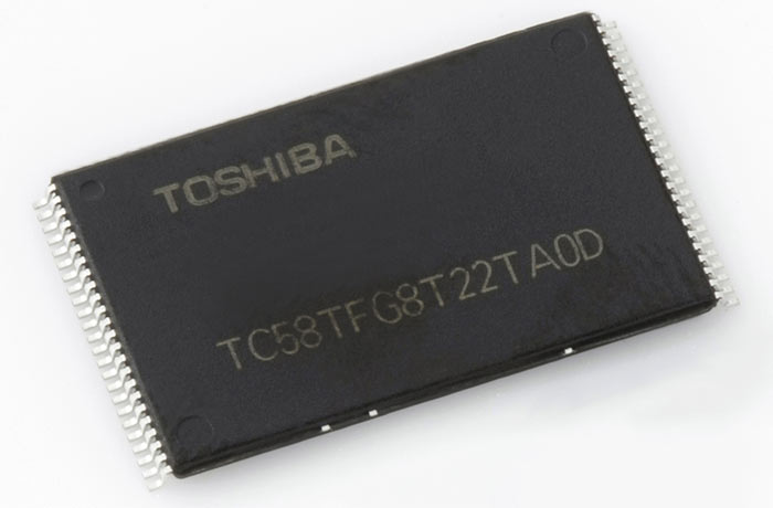
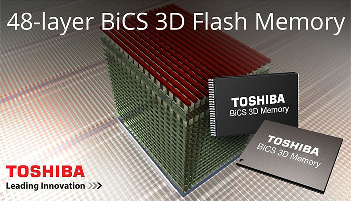
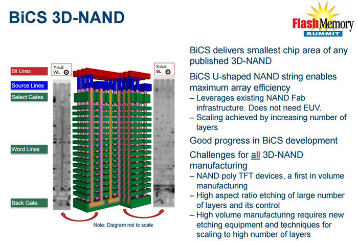
Toshiba and SanDisk have unveiled a new generation of BiCS (Bit Cost Scaling) FLASH memory. This new 3D NAND will be the world's first 256 gigabit (32GB) 48-layer BiCS FLASH memory chip. Toshiba and SanDisk's latest chips will use 3-bit-per-cell TLC (triple-level cell) technology and are built with 15nm technology. The new chips represent a doubling in capacity in just a few months. Back in March Toshiba announced the first 128 gigabit (16GB) 48-layer BiCS FLASH non-volatile memory chips.

While the first samples of this new NAND will be shipped to manufacturers in September, it won't be until mid-2016 that Toshiba and SanDisk will be ready for mass production. In a press-release announcement from Toshiba, the company says that its Yokkaichi manufacturing operations Fab2 facility in Japan, where the new chips will be made, will be completed by that time.

Toshiba predicts that the new memory will be used in diverse applications including consumer SSDs, enterprise SSDs, smartphones, tablets, and memory cards. The new BiCS FLASH will help "support the storage market's demand for ever-increasing densities," said Scott Nelson, SVP of the Memory Business Unit at Toshiba America Electronic Components (TAEC).

Sandisk released a separate statement concerning the development. Dr. Siva Sivaram, executive VP, memory technology, SanDisk wrote "This is the world’s first 256Gb X3 chip, developed using our industry-leading 48-layer BiCS technology and demonstrating SanDisk's continued leadership in X3 technology. We will use this chip to deliver compelling storage solutions for our customers." Sandisk uses 'X3' to describe TLC memory technology.
In addition to its greater densities BiCS NAND provides enhanced write/erase endurance, write speeds and energy efficiency when compared to 2D NAND.


