Micron Technology has announced that it has started to sample next-generation NAND flash memory built using a 16nm process. The new process node will enable Micron to manufacture the world's smallest 128-gigabit (Gb) multi-level cell (MLC) NAND Flash memory devices. Micron says this technology "solidifies" it's leadership position in storage technology development.

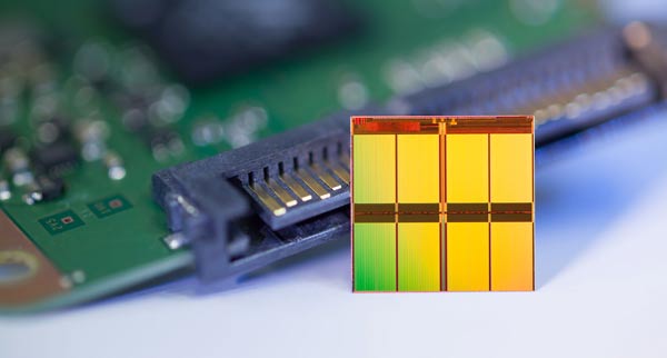
The new Flash NAND built at 16nm will be targeted for use in consumer SSDs, removable storage (USB drives and Flash cards), tablets, ultrathin devices, mobile handsets and data centre cloud storage. In reducing the size of the process Micron will achieve "the greatest number of bits per square millimetre and lowest cost of any MLC device in existence". This sounds good for further price reductions and larger capacity flash memory devices for we end users. 16GB of storage will be able to be provided on a single die, as pictured below.

Speaking about the process size reduction Glen Hawk, vice president of Micron's NAND Solutions Group, said "Micron's dedicated team of engineers has worked tirelessly to introduce the world's smallest and most advanced Flash manufacturing technology." He added that "Our customers continually ask for higher capacities in smaller form factors, and this next-generation process node allows Micron to lead the market in meeting those demands."
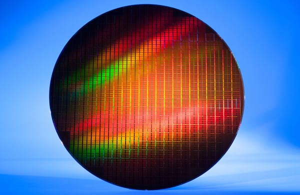
Micron includes a quote from Gartner which reminds us that "Cost reductions will always be fundamental to the NAND industry and so companies who can continue to lead on the flash process technology will be poised for success, particularly in vertically integrated solutions". Under the new process a single 300mm wafer, as pictured below can create nearly 6TB of storage (equivalent to ~ 1,300 DVDs).

Select partners of Micron are testing this 16nm, 128Gb MLC NAND now. It is thought that full scale production will start in Q4 this year. Furthermore Micron has voiced its intention to develop a new line of SSDs using the 16nm flash memory, which are expected to ship in 2014.


