facebook rss twitter

Intel, Micron announce first 128GB 20nm Flash NAND

by David Ross on 7 December 2011, 10:22

Tags: Intel (NASDAQ:INTC), Micron (NASDAQ:MU)

Quick Link: HEXUS.net/qabadg

Add to My Vault: x

Intel and Micron have created the first 128GB multi-level cell (MLC) NAND flash device developed using 20 nanometre (nm) processing technology.

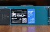
Under the name IM Flash Technologies, the two companies have also started mass production of 64GB NAND devices, created using the same process.

Offering twice the performance and capacity of the 64GB NAND, the 128GB device can store 1 terabit of data in a single tiny package with just eight die and can achieve speeds of 333 megatransfers (MT/s) per second


In a press release, Intel and Micron explained how they managed to create the flash devices using the 20nm process:

The key to their success with 20nm process technology is due to an innovative new cell structure that enables more aggressive cell scaling than conventional architectures. Their 20nm NAND uses a planar cell structure — the first in the industry — to overcome the inherent difficulties that accompany advanced process technology, enabling performance and reliability on par with the previous generation. The planar cell structure successfully breaks the scaling constraints of the standard NAND floating gate cell by integrating the first Hi-K/metal gate stack on NAND production.

The demand for high-capacity NAND flash devices is expected to grow over the coming years as demand for digital content and more effective storage in mobile devices increases. The two companies expect the two tiny products to be used in smartphones, tablets, solid state drives (SSDs), and other high-performance devices.

Intel and Micron plan to ramp up production of the 64GB flash product over the Christmas period and then make samples of the 128GB device available in January, followed by mass production in the first half of the year.


HEXUS Forums :: 6 Comments

Login with Forum Account

Don't have an account? Register today!
Wow…128GB on something as small as your finger-nail….that means that each 2.5" drive should be able to pack some amazing storage space….

Now, if only they managed to get cost of manufacturing down by an order of magnitude…… :P
shaithis
Wow…128GB on something as small as your finger-nail….that means that each 2.5" drive should be able to pack some amazing storage space…. Now, if only they managed to get cost of manufacturing down by an order of magnitude…… :P
+1 for this - although I'd gladly trade that TB+ 2.5“ drive for an affordably priced 500GB one - after all that's only 8 of those ”lesser“ 64GB modules (minus the usual allocation for bad cells etc).

Good side point though shaithis - if they can get storage that small, then is 2.5” necessarily a good format - perhaps time for something even smaller!?
Or….LARGER!

How many of those could you cram into a 3.5" drive? :devilish:
I just went to read the Intel press release (which I had to source from a well known tech blog owned by AOL as there wasn't a direct link from the Hexus article) to clarify if this is a 128GB part or a 128Gb part.

Intel
…the new 20nm monolithic 128Gb device is the first in the industry to enable a terabit (Tb) of data storage in a fingertip-size package by using just eight die.
So it would seam that the announcement is for a 128Gb part, but the chip in the picture is actually eight of these new dies in one package, making the picture a 128GB part.

http://newsroom.intel.com/community/intel_newsroom/blog/2011/12/06/intel-micron-extend-nand-flash-technology-leadership-with-introduction-of-worlds-first-128gb-nand-device-and-mass-production-of-64gb-20nm-nand

It's a rather confusing press release. To make it clear they should have a picture of a single die, and then the full package with eight dies balanced on the finger, not just one pic with a finger and one without.
shaithis
(Good side point though shaithis - if they can get storage that small, then is 2.5“ necessarily a good format - perhaps time for something even smaller!?) Or….LARGER! How many of those could you cram into a 3.5” drive? :devilish:
… more than I could afford! :help:

Actually, again that's a very good point, :thumbsup: how come that 2.5" seems to have become the standard SSD form factor? Yes, I know that means that you can sell the one part for desktops and laptops - but surely if you have a 3.5" box to fill then you could use lower density - cheaper! - modules. I admit that there's probably a physics based reason why more modules = slower response, but my woefully limited knowledge doesn't give it.