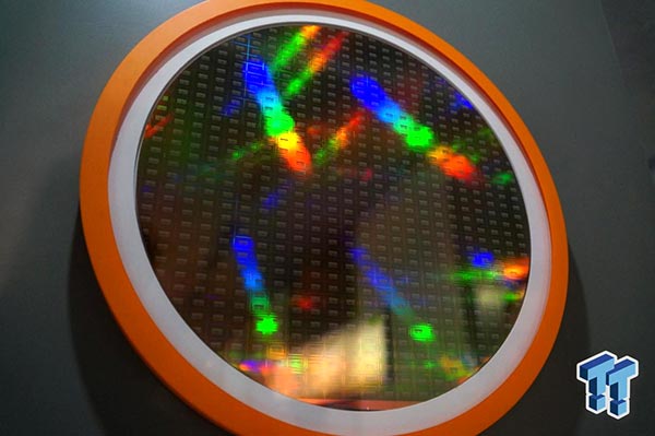
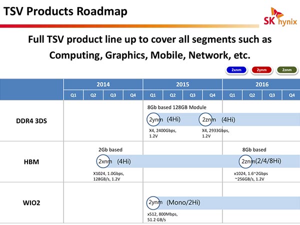
SK Hynix has been showing off HBM2, the next generation of its high bandwidth memory. The first generation HBM1 is expected to premiere on AMD Radeon 300 series graphics cards this summer. The second generation high bandwidth memory from SK Hynix will offer double the density and double the bandwidth of the first generation memory chips. It has been earmarked by Nvidia to form an important component on its Pascal GPU graphics cards in 2016.

As reported by Tweaktown, which took some pictures of an HBM2 wafer at the SK Hynix stand during the GPU Technology Conference this week (as above), the first and second generation HBM chips compare as follows:
|
|
HBM1 |
HBM2 |
|
Bandwidth per stack |
128GB/s |
256GB/s |
|
Chip density |
1Gb |
2Gb |
|
Voltage |
1.2V |
1.2V |
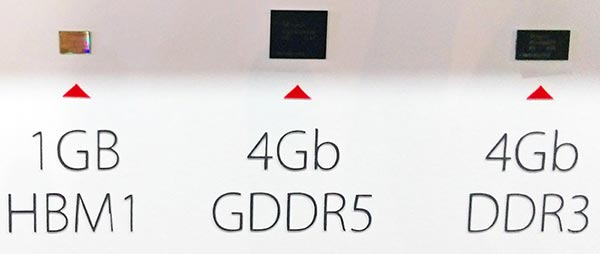
The greater density on offer with the HBM2 memory architecture will enable graphics cards with up to 32GB of RAM. The stacking of the memory chips using Trough Silicon VIA (TSV) technology enables HBM (1&2) memory chips to be much smaller. Fudzilla published a picture showing how much smaller 1GB of HBM1 memory is compared to 4Gb of GDDR5 or 4Gb of DDR3 RAM, see below.

AMD is set to gain a significant performance bonus from the adoption of HBM1 in its available graphics cards, it has got perhaps six months or more before Nvidia can strike back. While Nvidia may have already signalled it will skip straight to HBM2, by the 2016 launch of Pascal AMD may update its graphics card range to include this second generation HBM too.


