In December last year TSMC started to work on its 5nm process. In the following January we heard from the firm's CEO about the progress of these plans, with a target launch date set for H1 2020. Now a recent report suggests that TSMC is confident of reaching its previously publicised goals, as it has started to allocate between 300 and 400 R&D staff to work on developing its 3nm process.

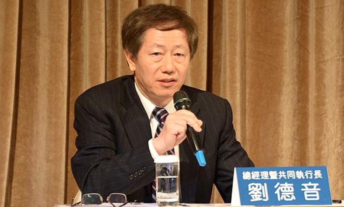
According to a report published by Taiwan's CTimes News, the large R&D staff allocation will work to "break the limitation of Moore's law and move toward the 3nm manufacturing process". Dr. Mark Liu, President and Co-Chief Executive Officer of TSMC told reporters that the tool to crack this particularly hard nut would be TSMC's three-dimensional stacked architecture technology.
Dr Liu said that TSMC has established "the complete ecosystems with the intellectual property, automation solutions and equipment providers," required to go forward and make Taiwan "the strongest fortress in the global semiconductor industry". Of course a big part of this succeeding in these efforts is investing in cutting edge technology and the amount and quality of R&D staff required to achieve the set-out goals.

If you think 3nm is ambitious and futuristic, Dr Liu has already earmarked the 3nm R&D staff to march onwards to 1nm process development. Such ambition and investment is important to TSMC, and to Taiwan, to maintain its leading position in the global semiconductor market.


