IBM announced its 7 nanometer and beyond research project almost a year ago to the day. This project kicked off with the expectation of requiring $3 billion in investment over the following five years. Now we hear that IBM has achieved a significant milestone in its progress to help it in the quest to create a processor that is at least two generations ahead of anything commercially available at this time.

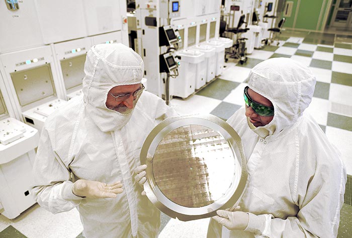
A 7nm chip wafer
The world's first 7nm chip with functional transistors has recently been produced by IBM with the aid of partners GlobalFoundries, Samsung, the State University of New York (SUNY) and others reports Ars Technica. It is claimed that this is the world's first "commercially viable" sub-10nm FinFET logic chip.
While IBM feared that 7nm chips might be out of reach, due to fundamental barriers of the technology used to create them, it leveraged innovations such as the use of silicon germanium (SiGe) alloy, channel transistors, and Extreme Ultraviolet (EUV) lithography at multiple levels to achieve its goal.
The result of the shrink from 10nm to 7nm is that there will be a 50 per cent chip surface area reduction and "at least a 50 per cent power/performance improvement" for these next-next-gen parts, according to IBM. The difference will be even more pronounced when compared to 14nm chips.

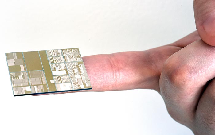
One of IBM's 7nm chips
Process shrinks have become increasingly difficult to achieve with commercial viability, and this fact is illustrated by the recent news concerning Intel's roadmap plan delay. Yesterday HEXUS wrote about how the 14nm Kaby Lake will be the successor to Skylake next year while the release of the 10nm Cannonlake slips further into the future. With this in mind it's pretty difficult to forecast when Intel's move to 7nm will come, but it should be roughly 2017/2018. Will IBM, GlobalFoundries and Samsung beat Intel to it?


