Here is some more interesting news from the GlobalFoundries Technology Conference (GTC 2017) in Santa Clara, California yesterday. One of the presenters from the chipmaking industry to take to the stage was none other than AMD's CTO Mark Papermaster. You can see the key presentation slide he shared at the event reproduced below. Importantly, Papermaster told attendees that AMD will be transitioning both graphics and client products from the 14nm LPP process to the new 12nm LP process during 2018.
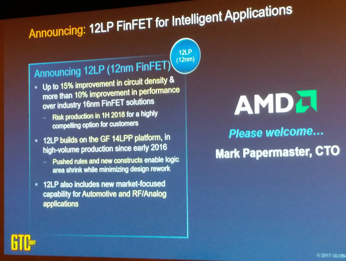
There's a lot of info packed into that slide above. While we wonder what material benefits will be delivered to AMD CPUs and GPUs from the move to 12LP, the comparison in bullet point one doesn't address this as it compares against "industry 16nm FinFET solutions" rather than the existing GloFo 14nm process that is used by AMD. Nevertheless there will certainly be some gains with minimal work needed to redesign by the engineers involved in the process. The final bullet point above touches upon the AMD / GloFo / Tesla collaboration, perhaps.
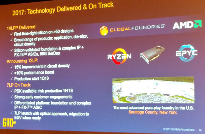
A subsequent slide, reproduced above, gives a better overview of the progress for the AMD and GloFo partnership. Here we can see that 12LP production will start in Q1 next year. Meanwhile, 7LP production will follow very shortly, within H1 2018 sometime.
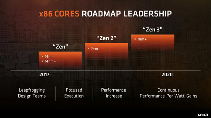
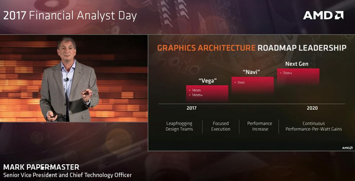
If you look at previously published AMD roadmap slides you can see that 7nm will usher in Zen 2 architecture x86 cores, and Navi architecture GPUs (click to zoom-in).
 |
 |