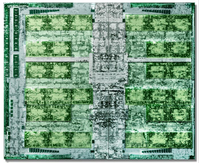
Nvidia showed off a close-up shot of the Pascal GP100 die at Hot Chips 28 this week. The suitably green hued 610mm2 chip is pictured in a clear magnified view, with various key functional component parts easily distinguished from one another.

The Pascal GP100 chip includes an impressive 15.3 billion transistors. In the die shot above you can see how various groupings are arranged around the chip design. Let's do an eye-spy of what we can see, in a simple bullet point list:
- 30 x Texture Processor Clusters – these are the darker green square areas, each TPC consists of two SMs (Streaming Multiprocessors). There's 60SMs in total.
- 4 x HBM2 interfaces – you can see these in pairs at the top and bottom of the die shot.
- 4 x NVLink interfaces can be seen on the left side of the die shot.
- In the middle 'spine' of the shot is the thread scheduler among other features.
AnandTech reckons that the GP100 is particularly interesting as it is the first Nvidia chip to feature HBM and NVLink components. The relatively small chip real estate taken up by the HMB2 interfaces is also commented upon.

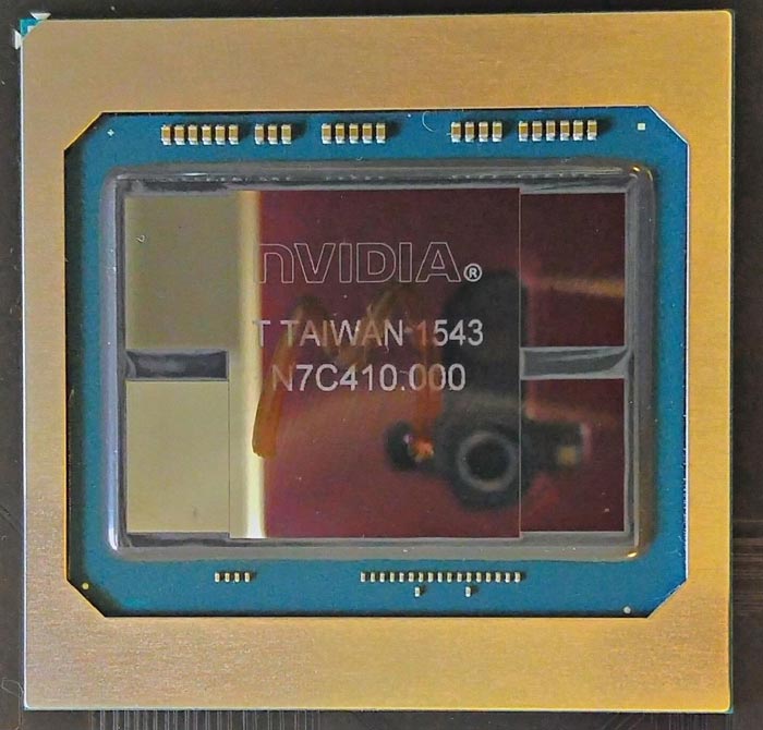
The Nvidia presentation complemented the die shot with a photo of a fully-clothed production GP100 package, above. As you can see the GPU and HBM2 stacks are very tightly packaged. The 4x HMB2 memory stacks added together (for 16GB of RAM) are approx two thirds the size of the GPU.


