The Memory Conundrum
One of the most common themes in modern GPU computing is the increasing reliance on memory both in terms of speed and size. The push to higher resolutions and rich textures is at loggerheads against the need to restrain memory power consumption which quickly spirals out of control when operating at sky-high frequencies oftentimes augmented with additional voltage.
The current status quo in the high-end GPU market is a compromise. GDDR5 memory, found on the latest GPUs from both Nvidia and AMD, runs at a maximum 7Gbps, or 8Gbps at a push, but adding a wider bus introduces design complexities that are not easy to solve. AMD's 512-bit bus on the Radeon R9 290X, for example, is designed in such a way as the physical on-GPU layers (PHYs) are small, but this has the eventual knock-on effect of reducing maximum frequency. Nvidia goes for a tried-and-trusted middle ground - a 384-bit bus interfacing with 7Gbps memory.
Both companies realise that allocating more power to regular GDDR5, thereby increasing bandwidth for those higher resolution and texture tasks, is an inelegant solution to a difficult problem. Having GDDR5 pull 40W at full chat affects how much computation power can be set aside for the GPU itself, particularly when considered against a standard 250W TDP. GDDR5 can be teased to provide more performance for this generation and the next, but the disproportionate relationship between DRAM bandwidth and escalating power needs to be overcome, even with the spate of recent bandwidth-saving techniques baked into the latest GPUs.
In an ideal world we'd need a memory technology that could provide oodles of bandwidth at a much lower energy cost than present GDDR5. Such memory would naturally provide the GPU more of the available TDP at its sole disposal, perhaps use far less board footprint through smarter design, and work with any modern processor, be it CPU, GPU or SoC.
The preamble brings us to a chat we had with Joe Macri, co-chairman of the memory governing body known as Jedec and technical guru over at AMD. It's no secret that the next high-end iteration of AMD's graphics is codenamed Fiji and is to be called the Radeon R9 390X when it makes an official bow in the next two months or so. The standout feature of this GCN-tweaked design is a new technology called high-bandwidth memory (HBM).
HBM to the rescue?
HBM is the next major innovation in DRAM memory and in its purest form drastically reduces power consumption and size by stacking DRAM slices on top of one another rather than having them individually placed around the GPU. Such an approach increases the bus width massively, takes away many of the archaic inefficiencies of regular DRAM and, well, is just a good egg from almost any perspective. Let's dive straight in.
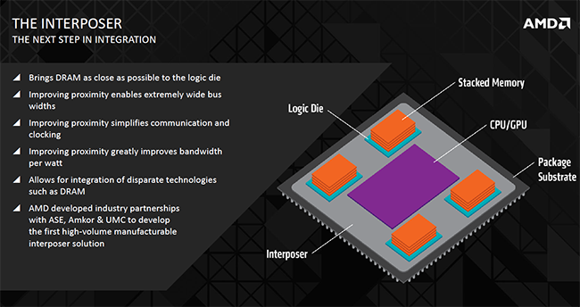
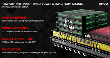
The premise behind HBM is to have memory as close to the processing unit as possible. Why? Because proximity to the workhorse enables very high bus widths to be achieved, signal paths to be kept shorter and some latency improvements to be gained as a direct result. The memory is connected to the GPU via an interposer, which in AMD's case will be composed of a simple silicon wafer. The interposer's job is to enable the processing units access to very wide bus widths that are not available on, say, GDDR5. How? Interposers can, and do, have significantly denser wiring than other connections - GDDR5 to GPU, for example - and its this innate denseness that enable the necessary bus width. But the real secret sauce is how the memory is stacked and the ancillary benefits that arise from it.
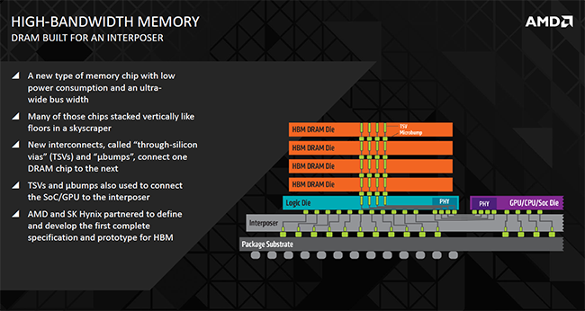
The interposer connects the GPU to a base logic die that acts as the go-between to stacked DRAM, and the very width of the connection makes HBM a viable solution at this juncture in time.
First-generation HBM will use up to four slices stacked on top of each other that are connected via technology called through-silicon vias (TSVs) and microbumps. 256 TSVs go through each slice making 1,024 in total. Bandwidth comes from the fact that each TSV can process 1Gbps in what is referred to in the industry as a Known Good Stacked Die (KGSD). Crunching the numbers shows that a potential 1,024Gbps is available from a four-hi-stack, or 128GB/s in common consumer parlance.
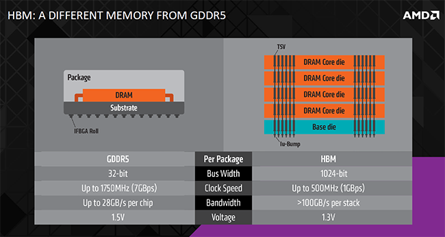
Here's a simplified view of HBM versus regular GDDR5 found on modern cards. HBM's proximity to the die and stacking ability offers an ultra-wide bus width alongside lower per-pin speeds. An added advantage is that operating voltage can be dropped, from 1.5V to 1.3V, further reducing power consumption.
So rather than use multiple GDDR5 modules to build up bandwidth via a collection of narrow buses that take up room on both the PCB and the die, HBM offers better-connected access through an externally wide bus linked via the densely wired interposer. Think of HBM as doing memory connections properly.
Smaller is better
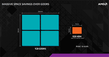
The very stacked nature of the DRAM has, as mentioned previously, the enviable benefit of reducing the memory footprint on the PCB. AMD reckons the size reduction compared to GDDR5 can be as much as 94 per cent while power efficiency increases massively, from approximately 10GB-per-watt on GDDR5 to 35GB-per-watt on HBM. The power savings can then be recirculated to the GPU for extra in-game performance. A 3x improvement from clever engineering is certainly not to be sniffed at. What's more, removing some of the older memory logic from the die, per GDDR5, paves the way for AMD to add in extra processing horsepower instead. A win-win situation, if you will.
There's a wider bus, significantly smaller physical memory footprint enabling pint-sized cards in the mainstream market, markedly lower power consumption that will undoubtedly play well for thermally-constrained environments, and reasonable bandwidth. What's the catch, you might ask, as we did to Joe Macri, because the sum of benefits appear too good to be true.
'HBM is very, very difficult to do properly, significantly more so than the already-complex GDDR5,' Macri said, alluding that AMD had been working on this memory problem for the best part of seven years, many of those with industry giant Hynix. 'Good engineers are lazy engineers,' he said, because spending the right amount of time on technology now will save inordinate time in the future.
Perhaps more prosaically, having a lead in memory architecture enables AMD to take some of the pressure off the GPU core. It was first with GDDR5 memory, with Nvidia coming to market substantially later, a point which Macri was keen to illustrate. HBM looks like it will follow a similar path as AMD takes the bulk of the R+D risk to eke out extra performance through lower power and a cleaner architecture.
Going by Macri's bullish outlook, AMD has apparently solved the HBM design and implementation problem that will eventually fall to all who need to use memory for processors. The implications are far-reaching, from Nvidia to Intel to ARM, but, right now, HBM may not quite be that appetising free lunch it first appears.
So what's the immediate catch?
Memory partner Hynix has openly stated that first-generation HBM will use 2Gb slices resulting in 256MB on each of the four-hi-stack modules. That's a total of 1GB per stack or 4GB for the four supported stacks. This means, quite clearly, the Radeon R9 390X, the first recipient of HBM memory, will very likely have 4GB of HBM memory, not 8GB or a Titan X-matching 12GB.
Whether the presumed 4GB framebuffer limit is going to be a big issue is up in the air. We've known for some time that playing games at high resolutions and high image-quality settings hammers the framebuffer sufficiently for many GPUs to scuttle off and use the slower PCIe bus and main system memory. Recent marketing shenanigans have pointed to 8GB and 12GB as the required framebuffer space moving forward. Indeed, we polled our knowledgeable audience about this very topic recently, and most erred between 4GB and 8GB.
Joe Macri's response on whether the 4GB framebuffer will cause consternation for what is a very high-end GPU was predictably pragmatic. 'We need to educate games developers to optimise for a reasonable amount of memory,' he said, intimating that 4GB was plenty, if used properly and efficiently, for the usage scenarios of a high-end graphics card. Second-generation HBM increases both speed and capacity thereby mitigating this immediate problem.
HBM has clear advantages over regular GDDR5 because it's purposely designed to remove the long-standing inefficiencies that have been part of the graphics card fabric for years. Way smaller, considerably more power efficient and with a firm roadmap for scaling, HBM will become the mainstream choice for all manner of processors in time. Whether it's an immediately good fit for the R9 390X remain to be seen, but AMD is doing what it does best, pushing the innovation boat out at the earliest opportunity.


