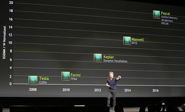
During a keynote speech at the annual Nvidia GPU Technology Conference in San Jose, California, CEO Jen-Hsun Huang showed off an updated (public) GPU roadmap. The headline announcement was of 'Pascal', the GPU family which will follow this year's Maxwell GPUs. Pascal GPUs are scheduled for launch and roll out in 2016.
The new GPU range, named after the 17th century French mathematician Blaise Pascal, weren't just name-checked. Nvidia also let us in on some of the key technologies which will be employed by Pascal GPUs to achieve more performance. The main advances to be present in Pascal were sketched out in four bullet points by Nvidia, as reproduced below:
- 3D Memory: Stacks DRAM chips into dense modules with wide interfaces, and brings them inside the same package as the GPU. This lets GPUs get data from memory more quickly – boosting throughput and efficiency – allowing us to build more compact GPUs that put more power into smaller devices. The result: several times greater bandwidth, more than twice the memory capacity and quadrupled energy efficiency.
- Unified Memory: This will make building applications that take advantage of what both GPUs and CPUs can do quicker and easier by allowing the CPU to access the GPU’s memory, and the GPU to access the CPU’s memory, so developers don’t have to allocate resources between the two.
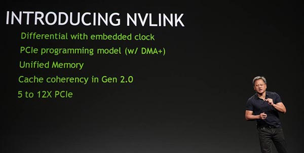
- NVLink: Today’s computers are constrained by the speed at which data can move between the CPU and GPU. NVLink puts a fatter pipe between the CPU and GPU, allowing data to flow at more than 80GB per second, compared to the 16GB per second available now.
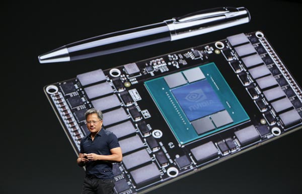
- Pascal Module: NVIDIA has designed a module to house Pascal GPUs with NVLink. At one-third the size of the standard boards used today, they’ll put the power of GPUs into more compact form factors than ever before.

Memory interface will be improved from hundreds to thousands of bits wide
You can see from the above that Nvidia puts a lot of Pascal development focus into the memory accompanying the GPU, both the memory structure/interface and the way that this memory is unified with the CPU memory pool. The 3D stacked memory will up the GPU interface from hundreds of bits to thousands of bits, stressed Huang in his keynote. The bandwidth will benefit from a "huge leap", just look at the chart below to see what will happen thanks this 3D memory and heterogeneous implementation.


Also to improve data transfer speeds inside your computer system Nvidia is proposing the NVLink chip-to-chip interface to replace the currently popular PCI-e 3.0 standard and offer between five and twelve times as much performance. This is a key part of the Pascal implementation and also allows modules to be produced which are a third the size of PCI express cards.

More details about the Pascal GPU line, including its architectural innovations, are promised for future revelations. As mentioned in the intro we have a long time to wait before we see Pascal hardware as it is scheduled for rollout in 2016.


