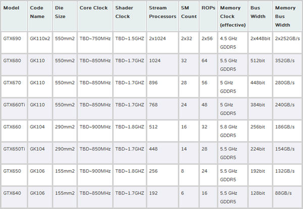
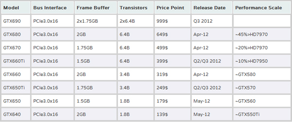
Details of NVIDIA's Kepler architecture still remain scarce, with many rumours considered to be propaganda and heavily unsubstantiated. Amongst these rumours are suggested release specifications, dates and prices for the Kepler line-up, released by LenzFire.


With no sources cited, we suspect these figures to be complete conjecture but is it possible to glean elements of truth from these tables? Certainly, press feedback from CES suggested a smug feeling of superiority from NVIDIA when asked about its concerns over AMD's first-to-goal Radeon HD 7xxx series, leaving us to expect much from Kepler, especially given its delayed release.
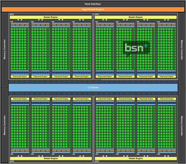
TechPowerUp has claimed that its information does in fact stem from "reliable sources" and suggests that Kepler's revamped CUDA architecture will focus on improved parallel performance, with an extra, and presumably cached layer at the top of the hierarchy, dubbed the Graphics Processing Cluster (GPC), with each cluster enclosing four Streaming Multiprocessor (SM) cores, with each SM containing 96 Stream Processors (SP).
This is in contrast to Fermi where SMs are not clustered, with the GTX 580 containing one third of the SPs per SM. This massive increase in Stream Processors follows somewhat with trend, as later dies in the 5xx series such as the GF114, GF116 and GF118 featured 48 SPs per SM. With TechPowerUp suggesting that there will be four clusters in the GK104-based 6xx cards, this would result in 1,536 CUDA cores, a three fold increase over the current generation. What's more is the site claims that the new design will feature twice the number of TMUs, with eight per SM.

All this points to an incredibly large die, with the added heat lowering possible clocks, with the site suggesting that CUDA cores will no longer function inside their own clock domain and will tick over at the same rate as the rest of the card, which looks to be 950MHz. If TechPowerUp's claims are legit, we'll soon be seeing cards with 2.9 TFLOP/s of single-precision floating point compute power and 486 GFLOP/s at double-precision.
The site's claims fail miserably to match up with the above figures, though TechPowerUp's claims of a 340 mm² die, 32 ROPS, 16 SMs per cluster and ~950MHz clock do support figures for the GTX 660, with the mistake, perhaps, that it would feature four clusters, where perhaps this configuration could be how NVIDIA intends to accomplish its high-end GK110 implementation.
Only time will tell but we wish that time would come sooner, as the suspense is too much to bear.


