Vega Design Philosophy
AMD is taking a two-pronged approach in wooing the enthusiast during 2017. You will likely have heard about the new CPU architecture, now known as Ryzen, which is designed to take Intel's premier consumer processors head-on. If what AMD promises turns out to be true, Ryzen puts the Austin company very much back in the high-end CPU game. We'll know more in the coming weeks, but there is room for AMD to be optimistic.
The other strand rests with new graphics solutions. Last year, AMD introduced the Polaris architecture, built on a leading-node 14nm process and providing renewed bang-for-buck for the mass-volume mainstream market.
Though Polaris continues to measure up well to what Nvidia has in the $100-$250 space, AMD, sagely, left the high-end market alone until it was ready to tackle it with a bigger, meatier architecture. The knock-on effect of such an approach was to leave that market to Nvidia, who has duly sewn it up with the premium 10-series GPUs such as the GTX 1080 and GTX 1070.
We've known for a while that AMD was cooking up a new premium architecture, codenamed Vega, and now we can reveal many of its architectural underpinnings before widespread launch in a few months.
Before we delve into the nuts and bolts, it is important to appreciate the underlying goals that AMD wants to meet with Vega. Raja Koduri, chief of the Radeon Technologies Group, described four current graphics-related bottlenecks and problems that AMD has attempted to meet with Vega, so we'll go through each in turn to see how the new graphics architecture meets them.
Addressing the Imbalance Between Compute and Storage
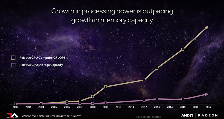
Koduri's first assertion was that the increase in GPU compute capability is far outpacing the available memory footprint, thus limiting the inherent potential of modern graphics accelerators. From huge game-install sizes to massive increase in compute workloads, modern GPUs, he said, need to able to transfer data from storage to the compute cores in a more efficient, faster manner. In other words, the GPU's framebuffer needs to be bigger, faster and have access to more virtual addressable memory space.
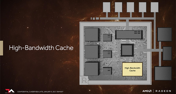
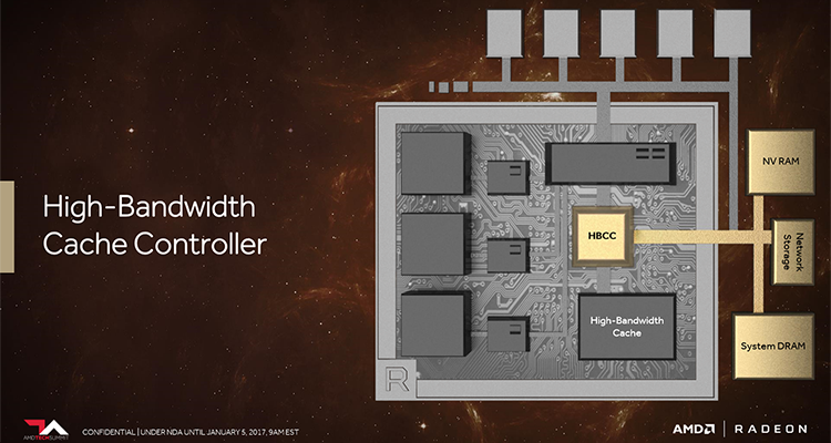
Vega, therefore, implements a high-bandwidth cache as part of its design. This is a fancy way of saying that Vega uses HBM2 memory and an improved controller for accessing huge amounts of data from regular VRAM and potentially other sources of memory such as main storage or NAND, as is the case with Radeon Pro SSG.
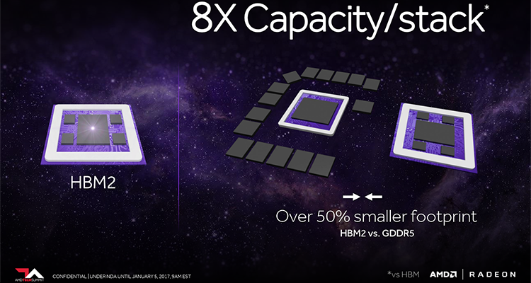
HBM2 has twice the bandwidth per pin as HBM1 and is able to be laid out in denser capacities due to die-stacking. As it stands, HBM2, in Vega form, will run at speeds of up to 2GT/s per pin, or 256GB/s per package, so double what you have already seen on the Fiji-based Fury boards. Running the numbers, expect Vega to offer 1,024GB/s of memory bandwidth in capacities of 8GB.
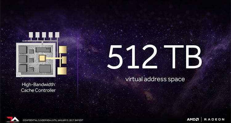
The second part is that the high-bandwidth cache controller can pull information from system memory and storage, offering more data to the GPU than just the card-mounted VRAM alone. Expanded to offer up to 512TB of addressable space, AMD says that speeding-up this part of the system is crucial in instances where Vega is deployed in a professional environment. Though no hard and fast numbers were shown in reference to previous architectures, AMD did demonstrate an application whose TB-sized datasets were being accessed in real time during 3D modelling.
A last word on memory. AMD intimated that Vega's memory-allocation system will be better than previous generations. Noting that in a gaming environment the amount of memory allocated to a game running at a high resolution is often far in excess of what it actually needs, smarter framebuffer algorithms should reduce the amount of RAM access Vega has to make compared to, say, Fiji.


