Semiconductor company Micron Technology, Inc. has announced that it has started shipping 2GB Hybrid Memory Cube (HMC) engineering samples to its lead customers. The firm says that HMC “represents a dramatic step forward in memory technology”. Initially it is envisaged that this tech will be employed in enterprise and corporations within data packet processing, data packet buffering and processor accelerator systems. However, within three to five years this HMC technology is expected to filter down to consumer applications.

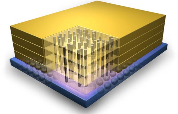
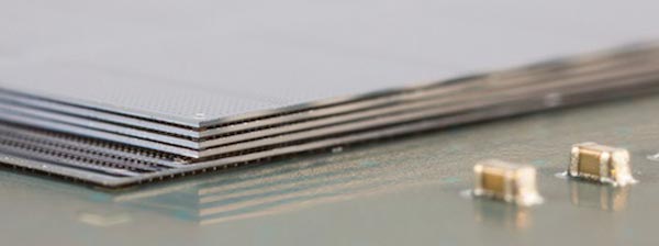
How does an HMC work? The DRAM memory chips are structured in a stack connected by vertical conduits combined with high-performance logic. This first 2GB engineering sample uses a stack of four 4Gb DRAM die. This cube memory structure provides around 160GB/s bandwidth, it also uses up to 70 per cent less energy than existing tech.
ComputerWorld magazine offers up a quote from Micron’s Mike Black, chief technology strategist for Micron's Hybrid Memory Cube team, explaining why this new memory is such an important breakthrough; “For quite some time memory and logic was tracking well, following Moore's Law. But, as the processor market took a lead in performance, we started falling behind in trying to keep up with improvements generation over generation. Processors with multiple core were being starved for memory.” HMC hopes to rectify that situation and be much thriftier in its power consumption.

The HMC specification has the backing of a hundred other tech companies with Micron, as well as Hynix and Samsung readying to produce this three dimensional RAM. Micron says that the current 2GB samples will be joined by 4GB samples early in 2014 with mass production of both sizes due to start later next year.


