After several weeks of leaked photos and details, we may finally have a complete set of information on NVIDIA's upcoming GTX 580.
The latest rumours from eNet in China seem to confirm the commonly held belief that the latest Fermi GPU will benefit from a full complement of 512 Cuda cores and 128 texture units. This will be hooked up to the same 384-bit memory interface and 1.5GB GDDR5 found on the current crop of GTX 480s.
Core specs are all good and well, but it's the clock speeds that complete the picture. The GPU itself is rumoured to be set to 772MHz, which translates to a 1,544MHz shader clock, while the memory will run at 4,008MHz. This compares to 700MHz, 1,401MHz and 3,696MHz for the GTX 480, representing a boost of about a ten per cent.
With more active components in the core and higher frequencies that its predecessor, you'd expect power draw to go through the roof, but apparently NVIDIA's engineers have actually managed to lower the TDP. The source suggests that new card will be rated at 244W - six watts less than the GTX 480 - showing just how much more efficient the redesigned core is. However, this is still slightly higher than the rumoured 225W power-draw of AMD's Radeon HD 6970.
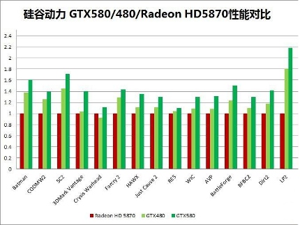
So what does all of this add up to in performance terms? A post on PCOnline claims to have figures comparing the new card to the current top of the line GPUs from AMD and NVIDIA. Though it varies, frame rates on real world tests average around 30 per cent higher than the HD 5870 and ten to 15 per cent higher than the GTX 480. This is less than what had previously been rumoured, but more in line with what you'd expect from the modest clock speed and architecture improvements.
Obviously this is all conjecture, but we shouldn't have to wait too much longer to find out for ourselves - the GTX 580 is expected to launch sometime in the next few weeks, just before the HD 6970.


