facebook rss twitter

Researchers develop 3D imaging chip small enough for mobiles

by Mark Tyson on 6 April 2015, 11:35

Quick Link: HEXUS.net/qacqiw

Add to My Vault: x

Researchers from the California Institute of Technology (Caltech) science and engineering research and education institution have developed a tiny new 3D imaging device. The Nanophotonic coherent imager (NCI) device may hold the potential to allow device makers to implement 3D scanners in smartphones or wearables without significant cost.

The technology used by the imaging device to capture the 3D image data is based upon LIDAR (Light Detection and Ranging). Caltech's NCI illuminates an object with peak and trough wavelength aligned 'coherent light' and analyses the light waves being reflected by the object to create models with height, width, and depth information.

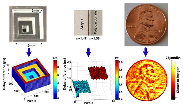
The NCI in testing was very small, less than a millimetre square, says Engadget. It only contained a 4x4 array of coherent pixels so can only scan small items right now. Even with the small coin, as pictured, it needed multiple passes to capture a complete scan. However it is impressively accurate down to 15μm depth resolution and 50μm lateral resolution (limited by the pixel spacing).

The Caltech researchers say that it would be easy to scale up the sensor with hundreds of thousands of pixels. This NCI could, in the near future, suit a diverse range of tech which would make use of precise 3D imaging from scanners associated with 3D printers, bio-medical imaging, security, robotics and self driving car sensors.


HEXUS Forums :: 4 Comments

Login with Forum Account

Don't have an account? Register today!
To scan my girl's ass or what? Damn, these science guys are really, really bored.
If it's less than a millimetre square, why does the image above show it's 10mm?

Wonder how many passes it took to create the coin image?
The depth resolution looks great though.

If scaling it up is as easy as they say they should release a much higher resolution version just to really show it off at it's best.
Odeas
If it's less than a millimetre square, why does the image above show it's 10mm?

That's not the sensor, that's an object scan: the object is 10mm across.
This basically replaces the switched pixel binning the Kinect 2's ToF phase sensor uses with spatial binning (i.e. the pixels are ‘stepped’ 1/2 a wavelength behind each other but capture at the same time). The 10mm structure pictured is a single ‘pixel’, of which an array would need to be produced to form a depth-sensing camera.

Unfortunately, it would STILL need temporal binning in order to sense depths deeper than the sensor itself. Great for very near field sensing like with the coin (sensor passes right over the surface), but if you want to do remote depth sensing you'll end up with depths ‘stacked’ into a repeating sequence a few mm thick.