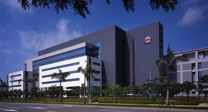
In a supply chain management conference earlier this month TSMC CEO Mark Liu said that his company had started work on a 5nm process node. At the conference, which took place in the TSMC HQ in Hsinchu, Taiwan, Liu discussed the move to push ahead with this most advanced technology yet but noted that TSMC is yet to decide whether to adopt extreme ultraviolet lithography (EUV) at the 5nm node.

If you take a look at TSMC's Future Major Project roadmap you can see 5nm transistors mentioned in the 'long-term research' category, spanning an estimated target schedule period of 2014 - 2019. You will see that running concurrently is TSMC's 'More than Moore' technology research where it endeavours to trial EUV and multiple e-beam tech to run ahead of Intel's famous electronics rule.
According to a report on the conference by The EETimes, the start of work on the 5nm process could indicate that "a combination of 193-immersion and EUV may be the best solution for the 5nm node as the semiconductor industry pushes the limits of Moore's Law". It explains that a 193i approach would be the most expensive but the EUV approach relies on immature technology.
TSMC 7nm node initial production expected in 2017
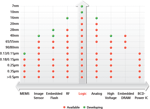
TSMC said that it had produced fully functional SRAM chips at 7nm in October. It expects production of chips at 7nm in volumes to start in 2017. The EETimes reports that TSMC "will begin technology qualification for 10nm during the fourth quarter this year, and customer tapeouts will start early in 2016".

Looking at the competition, IBM announced it had made the first "commercially viable" sub-10nm FinFET logic chip back in July this year. Big Blue used silicon germanium (SiGe) alloy, channel transistors, and Extreme Ultraviolet (EUV) lithography at multiple levels to achieve its '7nm and beyond' goal.


