Intel has announced to an investment of $4.1 billion in Dutch semiconductor equipment maker ASML. The aim of the investment is to gain technology that will accelerate the miniaturisation of computer chips and keep Intel at the forefront of competitive microchip technology.
The $4.1 billion deal consists of a $1 billion commitment to ASML’s R&D program and a 15 per cent stake in the company as a whole which will cost $3.1 billion. Initially the deal is only for a 10 per cent stake with the full 15 per cent being bought dependent upon shareholder approval. Veldhoven based ASML had previously stated that it planned to sell up to 25 per cent of equity to other chip makers to raise capital.

EUV lithography
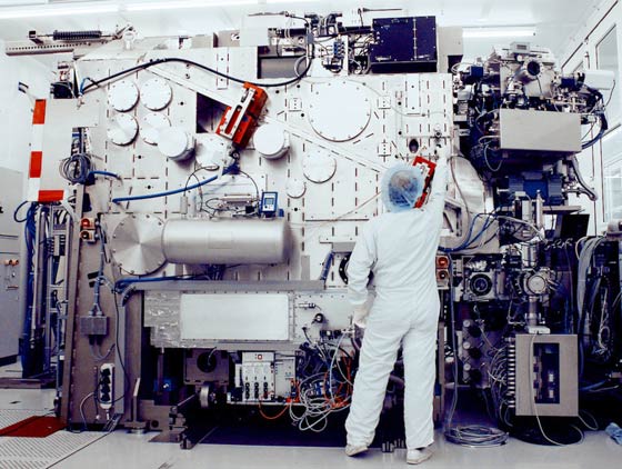
ASML is a leader in extreme-ultraviolet (EUV) lithography, a technology that has emerged as the industry’s best opportunity of maintaining Moore’s Law. EUV should facilitate the reduction in process size of chips to 10nm and below. Currently EUV circuit printing technology is too slow to be considered for mass production and a proportion of the R&D spend will be on improving this key manufacturing performance area along with process size reductions. ASML has stated the EUV process will be up-to-speed to be able to mass produce chips below 20nm by the start of 2013.
ASML say that EUV lithography will bring a lot of benefits “With the successful introduction of EUV lithography in high-volume manufacturing, multiple processing steps on critical layers can be eliminated on advanced manufacturing nodes, resulting in substantial manufacturing productivity gains, product power and performance enhancements, and lower capital expenditures.”
Wafer size transition
Another area that ASML will aid Intel is in the transition from 300mm wafer manufacturing to 450mm wafers. This move will increase output and reduce costs. Brian Krzanich, Intel senior vice president and chief operating officer said of the technology shift “The transition from one wafer size to the next has historically delivered a 30 to 40 percent reduction in die cost and we expect the shift from today’s standard 300mm wafers to larger 450mm wafers to offer similar benefits.”

Analyst Patrick Wang at Evercore Partners in New York spoke to the San Francisco Chronicle about the deal “Intel realizes they need 450mm sooner than anyone can give it to them. If they see a limit, down the road, which presumably they are, you could argue it’s a good use of cash.” The deal has the potential to accelerate Intel’s deployment of 450mm using EUV by up to two years.


