


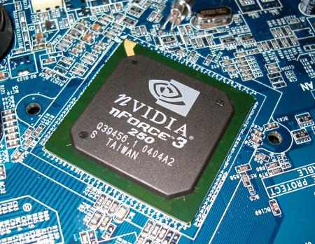
nForce3 250
The new chip comes in a variety of guises depending on the market segment a board maker wishes to target. There are versions aimed at compact or mobile implementations which feature on board graphics; nForce3 Go, which is already shipping. And then we have the versions aimed at drop in replacements for existing nForce3 150 designs, giving such boards a new lease of life with the new features. It's the 250 and 250Gb parts that will garner most attention from the online press and predictably that's what I'm looking at today.
The Gb part differs only in its implementation of a Gigabit Ethernet MAC and companion PHY (physical interface), giving boards that use it a high-speed networking connection, for those oh so prevalent gigabit setups in the home. It's still £20+/port for good gigabit infrastructure just for the home market, but in NVIDIA's defence, in choosing to use such a feature as a differentiator in its product line, it's still nice to see it make an appearance.
So it's the base chip that I'm looking at today, sans integrated graphics of course. Here's the feature list with K8T800 Pro's feature set (with likely VT8237CE bridge pairing) for comparison.
| NVIDIA nForce3 250 | VIA K8T800 Pro | |
| CPU Support | All Athlon 64 and Opteron variants, on all sockets, including Socket 940, Socket 939 and Socket 754. Only nForce3 250Gb supports Athlon FX and Socket 939, plain 250 is Socket 754 only. | All Athlon 64 and Opteron variants, on all sockets, including Socket 940, Socket 939 and Socket 754 |
| Memory Support | CPU based support but board support for up to 16GB of connected memory per processor when using Opteron | CPU based support but board support for up to 16GB of connected memory per processor when using Opteron |
| AGP | 8X | 8X |
| Southbridge | N/A | VT8237CE |
| Audio | AC'97 compatible link | AC'97 compatible link |
| HyperTransport Frequency | 800MHz (1600MTs/sec), 1000MHz (2000MTs/sec) only on 250 Pro | 1000MHz (2000MTs/sec) |
| HyperTransport Bus Width | 16-bit upstream and downstream | 16-bit upstream and downstream |
| IDE | 2 ATA133 compliant ports, 4 devices | 2 ATA133 compliant ports from VT8237, 4 devices |
| IDE RAID | Ability to RAID ports with 0/1/0+1/JBOD | Ability to RAID ports with 0/1/0+1/JBOD |
| SATA | 2 native SATA150 ports, PHY interface for 2 more | 2 native SATA150 ports, PHY interface for 2 more |
| SATA RAID | Ability to RAID ports with 0/1/0+1/JBOD | Ability to RAID ports with 0/1/0+1/JBOD |
| Networking | 100Mbit/sec Fast Ethernet MAC (1000MBit/sec MAC on Gb version) | 100Mbit/sec Fast Ethernet MAC |
| USB | 8 USB2.0 ports | 8 USB2.0 ports |
| FireWire | None | None |
| PCI | Primary and Secondary PCI busses, 32-bit, 33MHz | Primary and Secondary PCI busses, 32-bit, 33MHz |
Just for kicks, it's built by TSMC on their 150nm process and uses 22 million transistors.
A scan down the feature table tells us everything we need to know. nForce3 250 has been admirably brought up to date on the features front, and with the advent of high-specification audio solutions appearing from a wide range of sources, that aren't too expensive to add to boards, the loss of SoundStorm from NVIDIA's nForce3 product line continues to be lamented. But the passing of time heals old wounds and it's not as bad as it used to be. While NVIDIA will seek to distance itself from the use of something like VIA's Envy24-series of ASICs on nForce3 250 production designs, in reality the high-end Envy24s would complement anything just now (when implemented to its fullest), NVIDIA's hardware included.
We get 800MHz HyperTransport driven clock on all nForce3 250 products. 1000MHz support only appears in the Pro version of the chipset, for future processors. Parity in the up and downstream bus widths was a given, along with AGP and PCI bus locking if board makers implement it.
After that, there wasn't much else to fix. The audio problem is somewhat resolved these days, addition of 1000Mbit/sec networking a nod towards what everyone else is doing, lots of USB an absolute necessity and upgrades to the bridge's ATA and SATA support are most welcome. The overclocked, bridged, SATA150 implementation in nForce3 150 is now a thankful afterthought.
With AGP8X nearing the end of its useful life, we expect, no demand, a fast, complete and stable AGP8X implementation. With it being delivered by NVIDIA themselves, we can assume that's the case.
So, there we have it: a decent second generation Athlon 64 chipset. But don't you get the niggling feeling that it's what nForce3 150 should have been in the first instance? You aren't alone.
HyperTransport
A quick word about HyperTransport. 1000MHz support is for future processors only, only available on the Pro version of the chipset. On Socket 754 it's likely to be disabled completely, since no 1000MHz-able CPUs will be launched on that socket at all. It's unlikely that board makers will equip Socket 754 designs with Pro anyway. The press kit is an interesting hybrid. Socket 754, 250Gb Pro and a special Model 3400+ from AMD that's able to run at 1000MHz HT frequency.So what's it like wrapped up in a physical implementation?


