


Maxwell...a new way
Something really new
Nvidia is today launching the GeForce GTX 750 Ti. This all-new GPU is designed to provide decent gaming performance at a 1080p (1,920x1,080) resolution whilst also focusing on energy efficiency in the process. Priced from $149 from the usual bevy of partners, let's roll out the Table of Doom™ and take a high-level overview of what makes it tick.
GTX 750 Ti
|
GTX 650
|
GTX 650 Ti
|
GTX 650 Ti Boost
|
|
| Die Code name | Maxwell GM107 |
Kepler GK107 |
Kepler GK106 |
Kepler GK106 |
| DX API | 11.1 |
11.1 |
11.1 |
11.1 |
| Process (nm) | 28 |
28 |
28 |
28 |
| Transistors (bn) | 1.87 |
1.30 |
2.54 |
2.54 |
| Die Size (mm²) | 148 |
118 |
221 |
221 |
| SM Units | 5 |
2 |
4 |
4 |
| Processors | 640 |
384 |
768 |
768 |
| Texture Units | 40 |
32 |
64 |
64 |
| ROP Units | 16 |
16 |
16 |
24 |
| L2 cache (KB) | 2,048 |
256 |
256 |
256 |
| GPU Clock (MHz) | 1,020 (1,085) |
1,058 |
928 |
980 (1,033) |
| GFLOPS | 1,389 |
812.5 |
1,425 |
1,587 |
| Texture fill rate (GT/s) | 43.4 |
33.9 |
59.2 |
66.1 |
| Memory Clock (MHz) | 5,400 |
5,000 |
5,400 |
6,008 |
| Memory Bus (bits) | 128 |
128 |
128 |
192 |
| Max Bandwidth (GB/s) | 86.4 |
80 |
86.4 |
144.2 |
| Power Connectors | None |
None |
6-pin |
6-pin |
| TDP (watts) | 60 |
64 |
110 |
134 |
| GFLOPS per watt | 23.15 |
12.92 |
12.92 |
10.75 |
| SLI | No |
No |
No |
Yes, 2-way |
| Current MSRP ($ USD) | 149 |
109 |
129 |
149 |
The GTX 750 Ti has been lined up against three GTX 600-series GPUs that have provided the backbone for Nvidia's mainstream discrete graphics cards during the past 18 months.
GTX 750 Ti draws the closest specification parallels with the GTX 650 Ti that was first released in October 2012. Very conveniently ignoring the first few lines of the table - you'll understand why a little later on - the two Ti GPUs use a different mixture of shaders and frequencies yet arrive at a similar GFLOPS throughput figure. The older GTX 650 Ti actually has a greater bilinear texture fillrate, however they're identical with respect to back-end setup, composed of a 128-bit memory interface connecting to GDDR5 memory running at an effective 5,400MHz.
Yet, barely believably, Nvidia is claiming that GTX 750 Ti is not only 25 per cent faster than GTX 650 Ti in real-world games, the die is 30 per cent smaller, and it uses about half the total board power.This magic trick of Dynamo proportions needs some explainin'. You see, such performance and energy-efficiency improvements, especially on the same 28nm process node, simply are not possible when using the well-refined Kepler architecture. What's needed is a new GPU microarchitecture that reworks all the inefficient nooks and crannies present in Kepler, adds some more mojo on top, and presents it, in the first instance, on mainstream GPUs. That microarchitecture is codenamed Maxwell and the GTX 750 Ti is the first-generation implementation of it.
Maxwell: a better fit for the mainstream
Nvidia says it is introducing desktop Maxwell first for the mainstream market because this is where volume GPU sales occur. It is hard to argue against such financial logic but it's decidedly underwhelming that, for enthusiasts, high-end Maxwell won't debut until an undisclosed date. Nvidia's patently content with the price/performance/manufacturing cost characteristics of Kepler-powered cards such as GTX 770, GTX 780, GTX 780 Ti and sees no reason to upset the status quo.
Maxwell makes sense for the mainstream market in two important ways. First off, even without resorting to a smaller manufacturing process, GM107's die is over 30 per cent smaller than what, on paper, appears to be a performance-comparable Kepler part. Secondly, part of Maxwell's appeal is its much-improved power-draw figure, which is substantially lower than Kepler's.
So why is Maxwell so much more efficient and powerful than Kepler, you may ask?
Maxwell: my better is better than Kepler's better
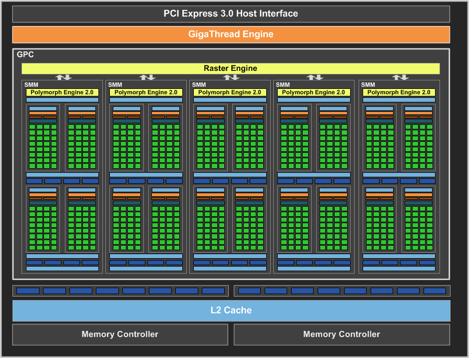
What you're looking at is the high-level overview of the full-fat Maxwell die present in the GM107 GPU. There's no major difference with respect to overall design - the setup engine feeds the graphics processing cluster (GPC) that in turn connects to a bunch of render outputs and to card memory.
The first key differentiator between Maxwell and Kepler is that Nvidia has redesigned the GPC. Maxwell's GPC houses five SM units instead of Kepler's three, though the shader/ALU count isn't too disparate as Maxwell drops the number of cores per SM down from 192 to 128. Crunch the basic numbers and Maxwell's GPC has 640 cores while Kepler makes do with 576.
The question then arises of why Nvidia made this change. It's all about improving per-SM efficiency, evidently. You see, Kepler architecture was first introduced almost two years ago with the arrival of the GeForce GTX 680. The intervening time has provided Nvidia's engineers with a number of methods for improving the design from a utilisation point of view - Maxwell, in a nutshell, is a major architecture overhaul of the Kepler base blueprint.
Improving the shader units
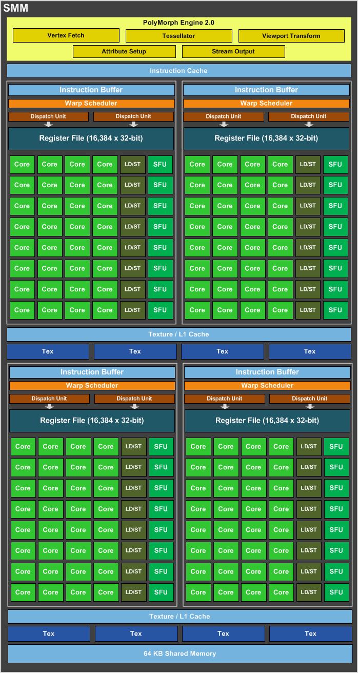
In Nvidia's own words '...the SM scheduler architecture and algorithms have been rewritten to be more intelligent and avoid unnecessary stalls, while further reducing the energy per instruction required for scheduling.' The statement is a tacit understanding that Kepler's scheduler was likely overloaded and not entirely efficient when arbitrating between 192 cores.
Take a peek at the SMM block (right) and Nvidia's realised it makes sense to split each SMM unit into, effectively, four sub-SM units. Each SMM now has four instruction buffers, register files, dispatch unit and schedulers, compared to one larger version for Kepler, and doing so saves die space and power.
Getting granular, Nvidia has now combined the texture and L1 caches into one (in contrast to Kepler) and 64KB of shared memory is now separate. Saving more die space, the ratio between cores and texture units now runs at 16:1, down from 12:1 on Kepler. This is why, as we alluded to earlier, Maxwell's texturing ability drops more than expected.
There's more to it than just this alone, too, as Nvidia removes a chunk of scheduling from the hardware and over to software (GeForce driver), thus following Maxwell's mantra of saving space, reducing power and increasing efficiency, according to Nvidia's representatives.
The sum of these high-level changes, and many behind-the-scenes improvements that Nvidia is not willing to talk about (improved circuitry, perhaps?), means that each of Maxwell's SMM units, whilst much smaller than Kepler's, offer around 90 per cent of their performance. Maxwell's SMM is doing almost as much as Kepler's SMX but uses considerably fewer resources and die-space to do so: a neat trick that is a boon for power consumption and enables Nvidia to squeeze more SMs in for a given silicon size.
What else can be done to minimise power usage and improve performance? Frequent trips to system memory are a sure-fire way to burn through juice, as any mobile phone or tablet manufacturer will readily attest to. Circumventing this problem as much as possible, Nvidia's increased the L2 cache from 256KB to a whopping 2,048KB, constituting an 8x increase. One would assume the larger die-space requirements must be offset by increased on-chip performance and lower power consumption.
And it's only on the front-end of a GPU that huge gains can be realised. The back-end - ROPs, memory controller, etc. - are largely similar to Kepler's. The mainstream GTX 750 Ti uses two 64-bit memory controllers in concert that connect to 16 ROPs. Somewhat mitigating the noisome effects of a narrow 128-bus is, one would presume, the 2MB of L2 cache and 2GB framebuffer.
Other improvements
Nvidia says it has also overhauled the NVENC video engine for Maxwell. This video-processor block provides up to 2x faster encode and 8x faster decode than the one present in Kepler, along with a new decoder cache that reduces power consumption.
Maxwell is also the recipient of a low-power state known as GC5, and its purpose is to minimise energy usage when the GPU is running basic tasks such as video playback.
In layman's terms, Nvidia has taken the well-performing Kepler architecture, squeezed and teased inefficiencies out of it via a major overhaul of the SMM units, shifted scheduling around, improved power consumption and built a leaner, meaner GPU. It reminds us of the microarchitecture transition between Intel's Ivy Bridge and Haswell processors, for whom driving down power consumption on mid-range parts was a key driving force.
The myopic focus on improving the performance-per-watt characteristic of Maxwell plays very well for TDP-constrained environments such as notebooks and very small-form-factor PCs. Nvidia is intimating Maxwell will give you approximately the same level of performance for half the power budget associated with Kepler, or about twice the performance for the same power budget. It's intriguing to imagine the kind of performance potential implicit in a second-generation Maxwell GPU, fabbed on a 20nm process, and rated with a 250W TDP: we guess that only time will tell.


