


Sandy Bridge improvements
AVX
Intel has a good habit of extending the feature-set of its processors through each generation. This means that, in broad strokes, the new chips provide a superset of features when compared to their immediate predecessors.
Sandy Bridge's superset involves providing general speed-ups that aren't based solely on increases in frequency alone. Intel's aim is to use specific hardware improvements to zero-in on making the processor more efficient. The first of these goes by the acronym AVX (Advanced Vector Extension), and it's an advanced form of the Streaming SIMD Extension (SSE).
In a nutshell, AVX doubles the chip's SIMD vector register from 128 bits to 256 bits and changes the format from XMM to YMM - the latter requiring operating system support. Further, AVX increases the two-operand instruction limit of SSE to three operands, which makes it easier for code to be written to the chip without having to destroy a register and therefore use up a temporary one. Less recycling, really.
Don't worry if this doesn't mean a lot to you, because the point of AVX is to make Sandy Bridge more efficient at processing the floating-point-intensive instructions used in applications such as image- and video-editing software, which rely heavily on SIMD optimisations.
Turbo Boost 2.0
The nominal frequency of a chip is fast becoming a poor indicator of the actual MHz speed. This is down to how both Intel and AMD have introduced core-based overclocking in their latest processors. Intel's technology goes by the name of Turbo Boost, as introduced in the Nehalem architecture in 2009. Turbo Boost 1.0 was good, but it's now being overhauled for Sandy Bridge...and with good reason.

Previous-generation Turbo Boost was based on controlling the CPU cores alone, at least for the desktop parts. Now, because the CPU and graphics portions are all on one die and total processor power is based on a combination of the two potentially operating in concert, Turbo Boost has needed an update.
The Turbo Boost logic contained within Sandy Bridge monitors the type of instruction that's being processed. Should it require some serious CPU grunt the cores ramp up, much like with Lynnfield chips, but with generally higher overclocks over the base speed. Here, though, the Turbo feature enables them to exceed the rated TDP for a short time. Intel is coy about exactly how long the chips can run past the TDP, but what's clear is that frequency is controlled by thermal power concerns, much akin to the latest high-end graphics cards from AMD and NVIDIA.
Furthermore, Turbo Boost 2.0 can be used to increase the speed of the graphics core when playing games. The premise here is to mete out more power when and where it's needed, though Intel, again, is reticent when defining exactly how the two Turbo Boost features work when both the CPU and GPU are taxed.
Beefed-up graphics
Speaking of the GPU and segueing serenely, Intel has improved the capabilities of the integrated graphics core.
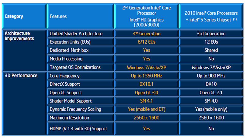
Here's a side-by-side comparison of Intel HD Graphics from the 2010 Core family (right) and the HD 2000/3000 Graphics contained within the Sandy Bridge chip.
Intel makes a big deal about the benefits arising from integrating the GPU on the same die as the CPU - citing reduced latencies, benefits of accessing on-chip cache, and finer control over the IGP's Turbo Boost features - but the real speed improvement comes by way of faster execution units and dedicated fixed-function logic.
The chip company also maintains that the new DX10.1-compatible units are simply clock-for-clock better than the older ones found in Clarkdale - well, it's hardly going to say they're worse, right? - and that the use of dedicated logic helps speed games along. Back-of-the-envelope calculations reveal that the Sandy Bridge IGP can be around 50 per cent faster than Clarkdale HD Graphics.
In keeping with the modular nature of the Sandy Bridge architecture and the firm's method of splitting it into the three Core divisions, the IGP can be comprised of either six or 12 execution units that can run at up to 1,350MHz. This leads to a lot of ifs, buts, and cans, granted, yet it's how Intel's marketing folk choose to differentiate. You'll need to keep a beady eye on the upcoming table to understand just how the IGP is split between models.
Media processor
But perhaps the most innovative part of Sandy Bridge graphics is the inclusion of dedicated logic for video decoding and encoding - the latter being fully-performed in hardware. Intel dubs this technology 'QuickSync Video' and has encouraged ArcSoft and CyberLink to release updates to video-editing apps that take advantage of this feature.
Akin to the UVD block in AMD hardware, the Multi-Format Codec uses a fixed-function architecture to speed-up computationally-intensive video processing, working, at times, in tandem with the GPU's shaders.
The IGP also supports post-processing effects such as video skin-tone correction and auto-contrast adjustment, though both NVIDIA and AMD have been doing this for a while now. There's also an update to the v1.4 spec of HDMI. If you've read any of our latest graphics-card reviews you'll appreciate that this means support for stereoscopic 3D.
Summary
Here are some takeaways for you. Intel controls around 80 per cent of the chip supply for the consumer market. It expects that the bulk of those sales will be composed of Sandy Bridge-derived chips in 2011, applicable to both the mobile and desktop segments. This fact makes the new architecture absolutely vital for the chip goliath's fortunes.
Intel has decided to look at increasing efficiency by rearchitecting the latest Core (2010) design. The CPU and much-improved GPU are inextricably mated on to one chunk of silicon, while a refined Turbo Boost implementation and new AVX instructions tap the potential of the core.
Sandy Bridge isn't representative of the huge shift that occurred when Intel launched the Nehalem core in 2008. Rather, a steady slew of improvements makes it difficult for existing OEM partners to look past Intel's line-up for both mobile and desktop parts.


