It was August when we announced that Samsung had achieved mass-production of 20nm flash that offered a significant performance rise to 1,500 and 3,500 IOPS read and write respectively, utilising the new eMMC 4.5 interface, allowing for simplified access at up to 200MB/s.
Though perhaps not holding the same significance to the future at Everspin's ST-MRAM, rather impressively, the firm has already begun mass-production of new 10nm modules, offering an improved 2,000 and 5,000 IOPS of read and write performance with speeds of 260 and 50 MB per second respectively, exceeding the specifications laid down by JEDEC's eMMC 4.5.
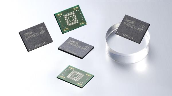
The flash modules come in 64Gb (8GB) sizes and have been dubbed the eMMC Pro Class 2000 (representing the read IOPS capability). It's Samsung's hope that this greater level of performance will see JEDEC create a new eMMC standard for the chips sometime next year.
Being compatible with the firm's previous 20nm process, Samsung has been able to deploy the new flash with productivity savings of 30 per cent whilst the chips themselves offer 30 per cent greater performance over their 20nm predecessors, with a 20 per cent smaller footprint.
Expect to find these units in high-end devices before the year's end.