


The burgeoning market for wearable technology is predominantly driven by chips based around the ARM architecture. Basic wearables, such as the fitbit activity tracker and Pebble smartwatch, typically use the ARM Cortex-M3 processor as the sensor hub, augmented by a Bluetooth controller usually based on ARM's lower-power Cortex-M0 technology.
Moving on up to premium wearables brings a wider range of ARM chips into play, with the more-powerful Cortex-A5 or Cortex-A7 harnessed as the brains behind the device, ARM Mali graphics, display processors and video engines for a richer visual experience on bigger screens, while the power-frugal Cortex-M0 pops up again as a sensor hub.
Point is, ARM is naturally keen to see the wearable market grow because it provides yet another opportunity for its partners - ST Microelectronics, Nordic Semiconductor, TI, Freescale, Qualcomm, et al - to cram in more processing cores. Got a wearable device? Chances are that it houses several processors built using ARM Cortex-A and Cortex-M IP. These in turn use real-time operating systems (RTOS) at the low-end and richer OSes at the mid- and high-end.
So with the combination of Cortex-A and Cortex-M playing such a big part in wearable technology, as well as widely prevalent in entry-level smartphones, it pays to understand their attributes better, particularly as they relate to device-specific implementations - Cortex-A7 in a wearable and Cortex-A7 in a smartphone are often markedly different beasts. But let's start with the itty-bitty Cortex-M first.
ARM Cortex-M
These processors are built with energy-efficiency very much in mind. Found in power-sensitive platforms and typically driving general-purpose microcontrollers, sensors and USB/Ethernet controllers, they're practically everywhere. Underscoring this point, scanners, networking, alarm systems, displays, power supplies, hard drives, white goods and medical devices, to name but a few, all use ARM Cortex-M-class technology, which is counted in billions of units per year.
Though designed by ARM to be highly configurable with respect to frequency and overall usage - ARM says there are more than 3,000 combinations of Cortex-Ms available from a range of partners - the utterly broad scope of use means ARM subdivides Cortex-M into four products.
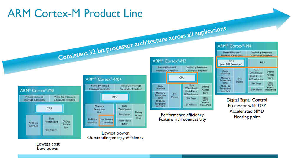
Shown as second in line, the Cortex-M0+ is the lowest-power CPU in the ARM arsenal. Based on the ARMv6-M architecture, it uses a two-stage, in-order pipeline and improves upon the Cortex-M0 by having an optional eight-region memory protection unit (also available on the M3 and M4) and a single-cycle I/O bus for, you guessed it, better power efficiency. It's also tiny with respect to size - 12,000 gates - and, as you will see a little later on, extremely good at sucking on miniscule amounts of juice.
The Cortex-M0, meanwhile, uses a slightly more complex three-stage pipeline, adding to the computational potential but also increasing power consumption a touch. The simpler design means it is the cheapest Cortex processor available, useful for general data processing and I/O control tasks. There's also a Cortex-M1, not shown, that's designed for FPGA chips.
Cortex-M3 and Cortex-M4 are bigger, faster CPUs primed for DSPs and and floating-point-intensive work. Both are based on the ARM v7-M architecture and can be frequency-scaled up to 200MHz, depending upon how fast a partner wants to make it.
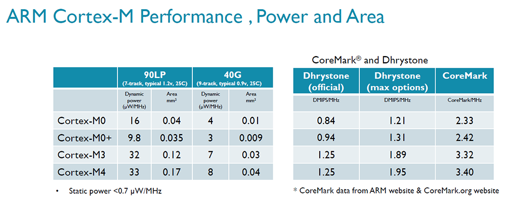
So just how small and power-efficient are they? ARM rarely divulges performance figures, purely because they're so dependant upon how a partner wishes to implement the cores, but these tables put the Cortex-M series into context.
Taken on a leading 40nm process, the Cortex-M0 pulls four microwatts for every MHz, dropping to three for the Cortex-M0+. That's crazy-low, frankly, as a microwatt is defined as one-millionth of a watt. Crunching the numbers shows that the Cortex-M0+ CPU core operating at 100MHz (which is relatively fast) uses one-ten-thousands of a watt. Perhaps even more illuminating is the tiny size of the CPU, measuring 0.009mm². Of course, the final chip, complete with caches, RAM, etc., is bigger, yet Freescale's Kinetis KL03's package, using a Cortex-M0+ running at 48MHz, measures just 1.6mm x 2mm - small enough to fit into the dimple of a golf ball.
Optimising ARM Cortex-A for wearables
Remember how we said that a Cortex-A CPU for smartphones and wearables can be an entirely different beast? ARM provides partners with guidance on how to implement its IP technology for a particular device, and it's much more than simply scaling the frequency and voltage back for wearable devices where, as you would expect, battery longevity is more important than all-out performance.
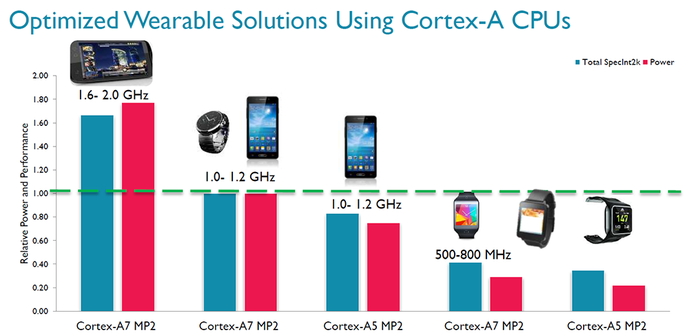
The graph has three instances of the Cortex-and-Mali combination powering mid-range smartphones, entry-level smartphones and smartwatches, respectively. The key takeaway here is that the Cortex-A7 can be purposely designed to be far more energy-efficient than expected when scaling down to wearables where, it is worth repeating, battery life is the most important criterion. So how is it done?
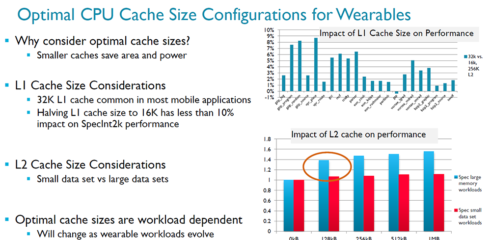
The modular nature of Cortex-A series design enables partners to custom-design their SoC to a large degree, especially for low power. Simplifying greatly, on-chip cache is good for performance but can be bad for power. Most smartphone SoCs using the Cortex-A7 equip the core with 32KB of L1 cache. Reducing this to 16KB, and therefore reducing both area and power, ARM says, does little to harm performance, particularly for a wearable.
Yet reducing the L1 brings cache misses more into play, thus putting the onus on L2. ARM says it's still worth partners using smaller L1 cache because the types of workloads executed on wearable technology don't show a great deal of performance degradation even when L2 cache is minimal. Designing for a wearable? Reduce the caches to save on power.
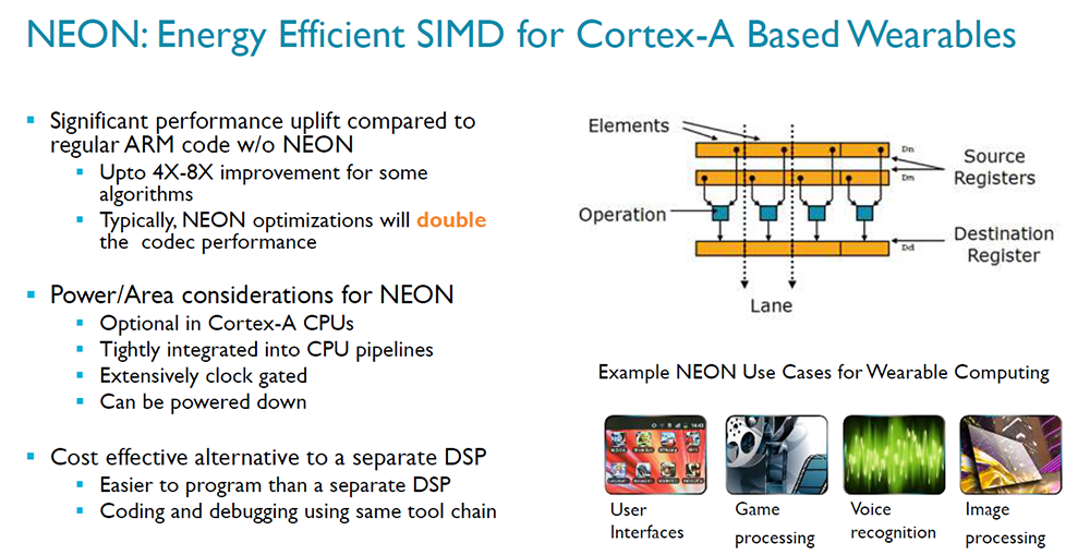
What else can a partner do? They could strip out the optional NEON SIMD engine to save even more space. This, however, is a false economy for all but the most basic of wearables, because the efficiency benefits and tight integration with the CPU core(s) outweigh the negative impact of increased die area and power.
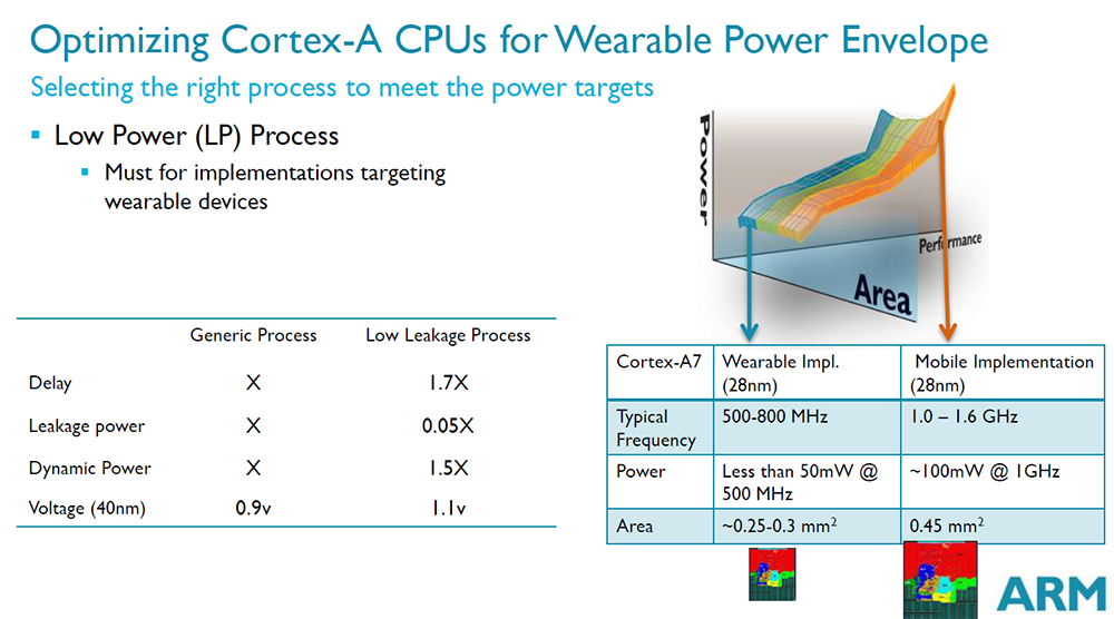
Then a partner can also deliberately choose an optimised, low-power process for fabrication. The ramifications of doing this are profound, as while frequency potential is curtailed - you cannot have high MHz and super-low leakage running concurrently - leakage, which is another name for wasted power, is reduced by a staggering 95 per cent.
Taking cache, architecture and low-power processes into account is a must when designing a wearable. The upshot is significantly increased efficiency and a smaller die than would be possible by simply scaling a standard-architecture Cortex-A series chip down.
ARM's modular design to IP enables partners to create super-custom SoCs that are suitable for a particular purpose. A Cortex-A7 in a smartphone can be very different to a Cortex-A7 in a wearable. Much like its nascent server strategy, there is no one-fits-all in the mobile space. Innovative and research-lead partners can make fundamentally better products than off-the-shelf designs.
We'll see the whole architecture behind wearables change as the devices themselves become more evolved. There's no magic bullet for increasing a smartwatch's runtime to weeks and months, but careful consideration of the workloads and architecture should enable manufacturers to eke out significantly more time between charges whilst not impacting on performance.


