Stanford scientists have developed 'high rise' chips that "could leapfrog the performance of the single-story logic and memory chips," in use today, reports Phys.org. The new approach, being pioneered by the scientists, sees chips being made with layers of memory sandwiched by layers of logic connected by thousands of nanoscale electronic 'elevators'. This new architecture, with its tight integration, promises faster, lower power computing.
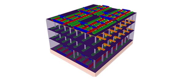
Central to the new architecture are three 'breakthroughs'; a new transistor fabricating technology, a new kind of multi-story friendly memory, and a 'radical' technique to join the new logic and memory together.
While the research is at an early stage Stanford professor of electrical engineering and computer science, Subhasish Mitra, says that the design and fabrication techniques employed are scalable. Mitra went on to assert that "With further development this architecture could lead to computing performance that is much, much greater than anything available today."
Supercomputer in your hand?
A prototype chip and supporting research paper will be revealed at the IEEE International Electron Devices Meeting (IEDM) in San Francisco later today. Another professor involved in the project, H.S. Philip Wong, claimed that "Paradigm shift is an overused concept, but here it is appropriate. With this new architecture, electronics manufacturers could put the power of a supercomputer in your hand."
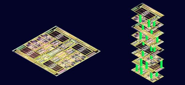
Single storey vs multi-storey circuits
The nanoscale 'elevators' mentioned in the intro have been made by very high performance carbon nanotube transistors (CNTs), built to span several layers of logic. The team has chosen to use resistive random access memory, (RRAM), which can be fabricated at much lower temperatures than silicon memory - aiding the production of the 'high rise' chips.
Phys.org explains that previous 3D stacking of silicon chips could save space but not improve interconnect speed as each layer was constructed separately and then connected via wires. The 'nanoscale elevators' through the new architecture can be much more numerous and direct and avoid 'digital traffic jams'. We are told that with the use of a commercial fabrication plant results should easily exceed the academic lab constructed prototypes.