


Programmable Geometry Pipeline
Successive GPU architectures don't tend to differ that much in their basic building blocks. Rather, in an attempt to eke out more, GPU architects tend to look at improving efficiency and doing more with the same number of shaders and back-end ROPs. And if you can get those shaders to operate at ever-higher speeds due to clever design, so much the better.
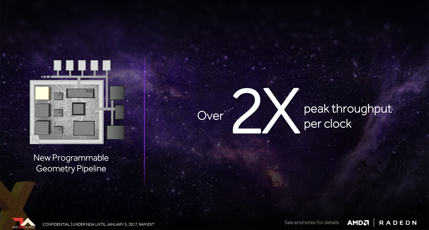
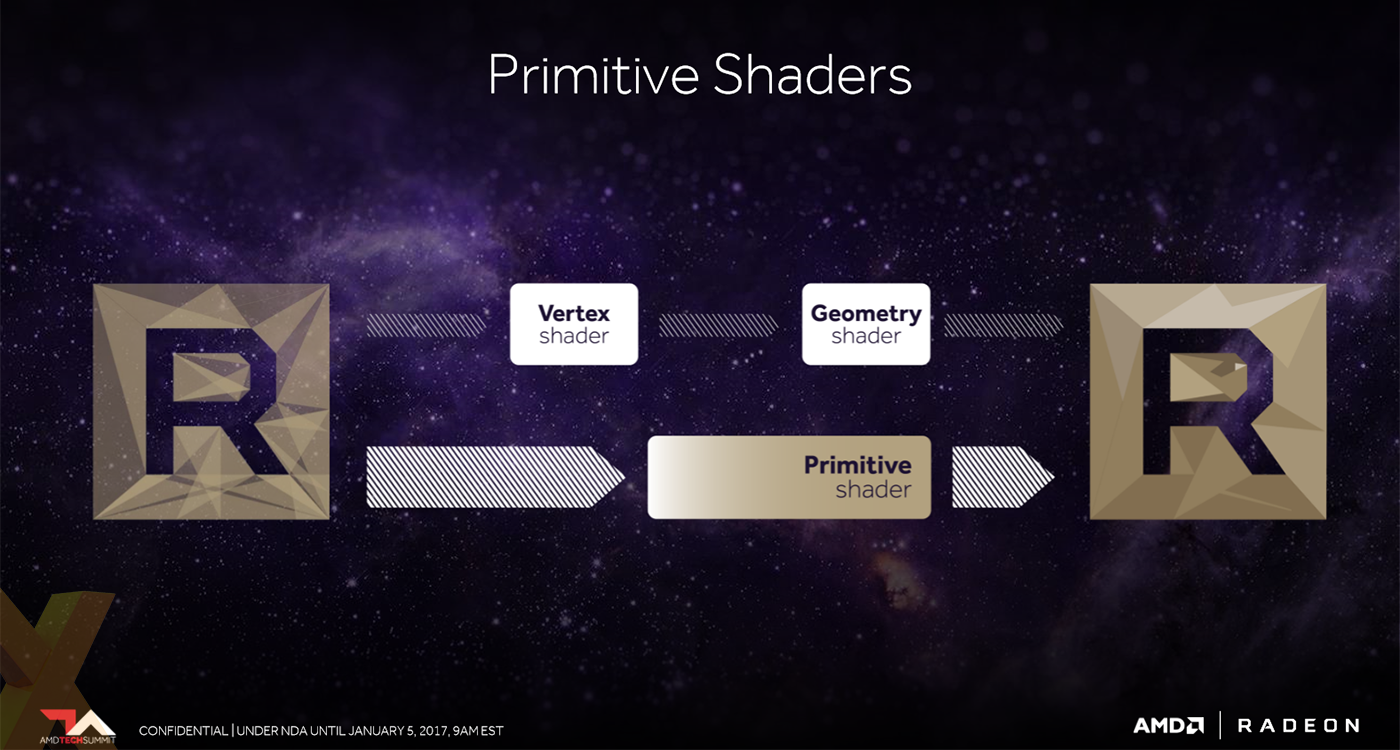
Examining the top end of the Vega architecture, Mike Mantor, AMD lead GPU architect, says that there is now more than 2x the peak geometry throughput per clock on this iteration. A traditional setup runs through both vertex and geometry shader, with the latter taking care of processing all of the vertices that make up the primitives. With Vega, according to Mantor, AMD is able to boost throughput by using a new stage in the pipeline called a dedicated primitive shader.
The point here is to allow developers to push the geometry work to a programmable shader, which, like computer shaders, should enable the GPU to better organise the work that it needs to do. In other words, it should be able to discard primitives that are never seen but still processed in a regular vertex-to-geometry setup.
And taking a leaf out of the console space, which AMD has solid knowledge of due its hardware being in both the Xbox One and PlayStation 4, a new workgroup distributor is added that looks at draw calls and overall processing to group things together for greater efficiency.
Arguably, the front-end setup of Vega is more console-like in nature, teasing out, on paper at least, the efficiencies those guys have already made.
Next-gen Compute Engine
Improving the front-end is fine but won't mean much if the powerhouse of the GPU - the compute engine - is left untouched. This part is what AMD refers to as the Vega Next-Generation Compute Unit (NCU).

We usually think of PC graphics architectures in terms of how well they process 32-bit (single-precision) operations. However, as a nod to how AMD sees the near-term future of graphics accelerators playing out, and how games and other applications will use various degrees of accuracy/precision, Vega offers 128 32-bit ops per clock, 256 16-bit ops per clock (half-precision), and 512 8-bit.
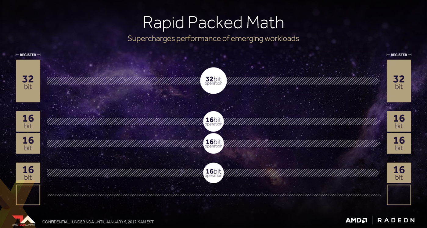
The less-accurate operations are becoming more interesting in some game rendering, and new, emerging workloads such as computer vision and pathfinding, says AMD, so it wants Vega to be a flexible mixed-precision architecture. Interestingly, the PS4 Pro is able to handle 16-bit ops simultaneously, and AMD uses what appears to be a similar technique, called Rapid Pack Math, for increased throughput on lower-precision workloads.
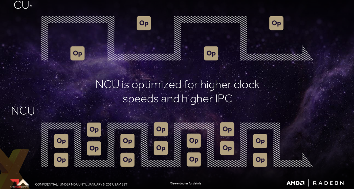
You know how Nvidia made great strides in increasing the per-core frequency on recent GPU architectures - we've seen close to 2GHz out of the box, helping the green team to some surprisingly high TFLOPS compute throughput through a streamlined design. AMD is taking much the same tack with Vega, by looking at all the critical pathways and removing bottlenecks, thus enabling thousands of shaders to work at, say, 1,500MHz or so. Without giving any of the actual sauce away, the company says the NCU is optmised for higher speeds and higher IPC. We'll know more about exactly how AMD achieved this closer to launch.


