Carbon nanotubes (CNTs) are lattices of carbon atoms rolled into tiny tubes. CNTs have excellent semiconductor properties allowing them to be used in making transistors. Until now, placing the CNTs closely and accurately was not possible so the technology applications in future computer chips implausible. IBM has announced that a team of its scientists has arranged CNTs 100 times more densely than previous efforts. The company has built a chip with 10,000 nanotube elements to test the fabrication process.
The IBM researchers are looking for a new way to make computer chips because the silicon technology we use today is looking to run out of steam. Intel’s current Ivy Bridge chips are made with transistor elements as small as 22nm and Intel sees the possibility to reduce the process as low as 5nm in the future but then some kind of revolution rather than evolution will be needed to make progress in line with Moore’s Law.
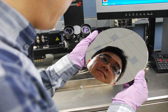 IBM researcher Hongsik Park looks over wafer with carbon nanotubes.
IBM says boldly “These carbon devices are poised to replace and outperform silicon technology allowing further miniaturization of computing components and leading the way for future microelectronics,” in its press release about the new CNT technology. The IBM researchers explain “Carbon nanotubes represent a new class of semiconductor materials whose electrical properties are more attractive than silicon, particularly for building nanoscale transistor devices that are a few tens of atoms across. Electrons in carbon transistors can move easier than in silicon-based devices allowing for quicker transport of data. The nanotubes are also ideally shaped for transistors at the atomic scale, an advantage over silicon.”
IBM reveals that its scientists have developed “a novel method based on ion-exchange chemistry that allows precise and controlled placement of aligned carbon nanotubes on a substrate at a high density”. The CNT density achieved is about a billion per square centimetre. The CNTs are dissolved in a soapy liquid and bond to well defined trenches of Hafnium Oxide on the chip substrate. “By combining chemistry, processing and engineering expertise, IBM researchers are able to fabricate more than ten thousand transistors on a single chip.”
This is an interesting development as CNT technology moves from being a “laboratory curiosity as far as microelectronic applications are concerned” to being a viable future contender to replace silicon chips.